GLT6400M16(2001) 查看數據表(PDF) - G-Link Technology
零件编号
产品描述 (功能)
比赛名单
GLT6400M16 Datasheet PDF : 13 Pages
| |||
G-LINK
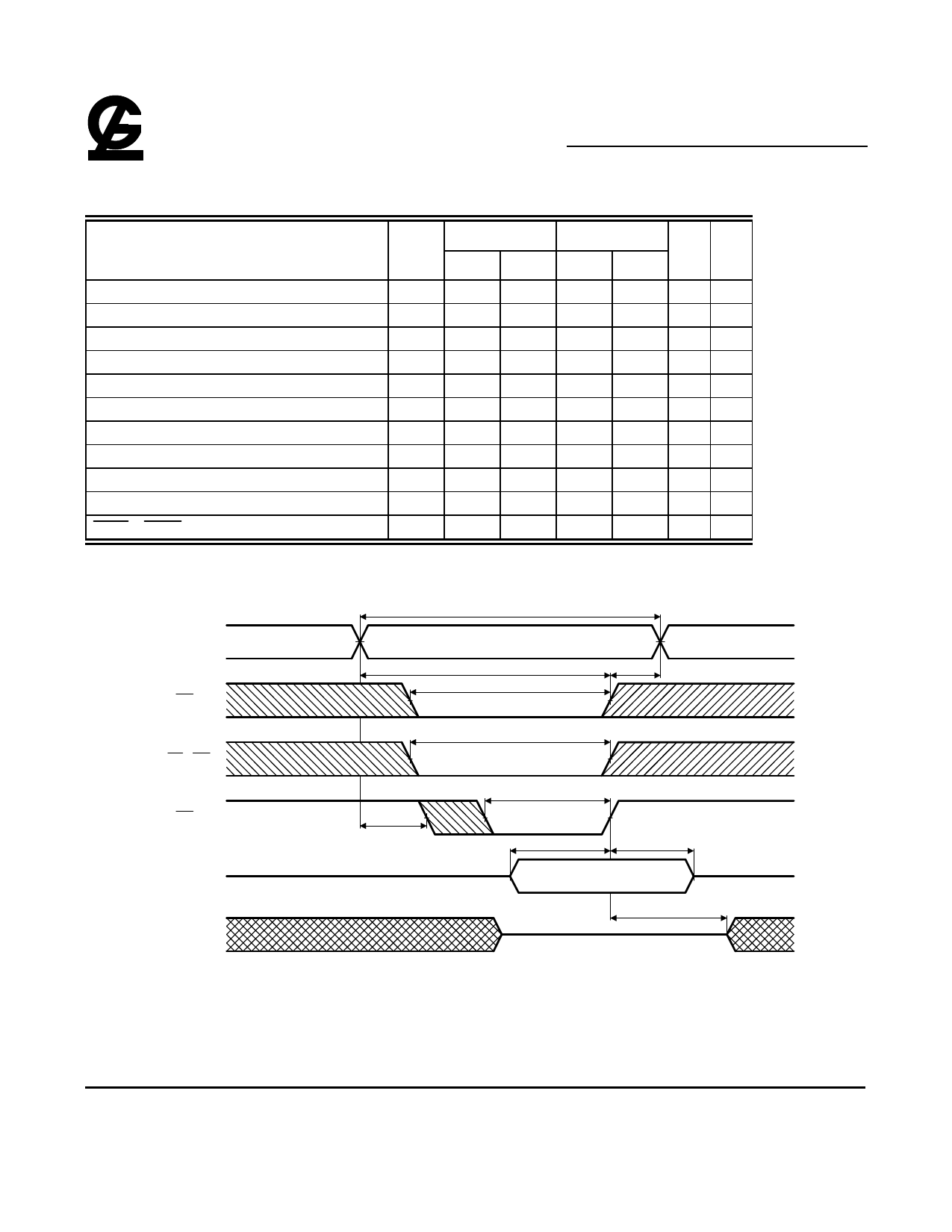
Write Cycle (11)( Vcc=2.3 to 2.7V, TA = -25°C to 85°C )
GLT6400M16
Ultra Low Power 256k x 16 CMOS SRAM
May 2001(Rev. 1.1)
Parameter
Write Cycle Time
Chip Enable to Write End
Address Setup to Write End
Address Setup Time
Write Pulse Width
Write Recovery Time
Data Valid to Write End
Data Hold Time
Write Enable to Output in High-Z
Output Active from Write End
BLE , BHE Setup to Write End
120
Symbol
Unit Note
Min Max
tWC 120 - ns
tCW 100 - ns
tAW 100 - ns
tAS
0
- ns
tWP 80 - ns
tWR
0
- ns
tDW 50 - ns
tDH
0
- ns
tWHZ
0
35 ns
tOW
5
- ns
tBW 100 - ns
Timing Waveform of Write Cycle 1 (Address Controlled)(2~6,8)
tWC
Address
CE1
tAW
tWR
tCW
tBW
UB / LB
tWP
WE
tAS
High-Z
DIN
tDW
tDH
DOUT
tOW
High-Z
G-Link Technology Corporation
2701 Northwestern Parkway
Santa Clara, CA 95051, U.S.A.
-7-
G-Link Technology Corporation, Taiwan
6F No. 24-2, Industry E. RD. IV, Science Based
Industrial Park, Hsin Chu, Taiwan.
Share Link: 