10XS4200 查看數據表(PDF) - Freescale Semiconductor
零件编号
产品描述 (功能)
比赛名单
10XS4200 Datasheet PDF : 60 Pages
| |||
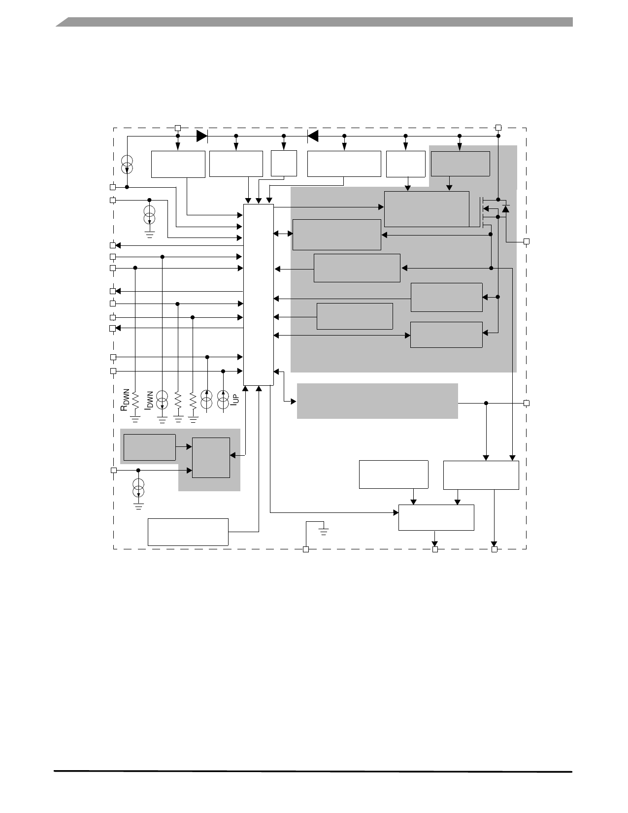
INTERNAL BLOCK DIAGRAM
VDD
INTERNAL BLOCK DIAGRAM
VPWR
CSB
SCLK
SO
SI
RSTB
FSB
IN0
IN1
FSOB
CONF0
CONF1
IUP
VDD Failure
Detection
IDWN
Internal
Regulator
VREG
POR
Over/Under-voltage Charge
Protections
Pump
Drain/Gate
Clamp
Selectable Slew Rate
Gate Driver
Selectable Over-current
Detection
Control
Logic
Severe Short-circuit
Detection
Over-temperature
Detect.
Short-circuit to
VPWR detec.
Open-load
Detect
HS0
HS0
CLOCK
Calibratable
Oscillator *
IDWN
VREG
PWM
Module
*
HS1
Temperature
Feedback
Output
Current Sense
Over-temperature
Prewarning
*blocks marked in grey have implemented
independently for each of both channels
GND
Figure 2. Internal Block Diagram
Analog MUX
CSNS
SYNC
HS1
10XS4200
2
Analog Integrated Circuit Device Data
Freescale Semiconductor
Share Link: 