APX9268 查看數據表(PDF) - Anpec Electronics
零件编号
产品描述 (功能)
比赛名单
APX9268 Datasheet PDF : 13 Pages
| |||
APX9268
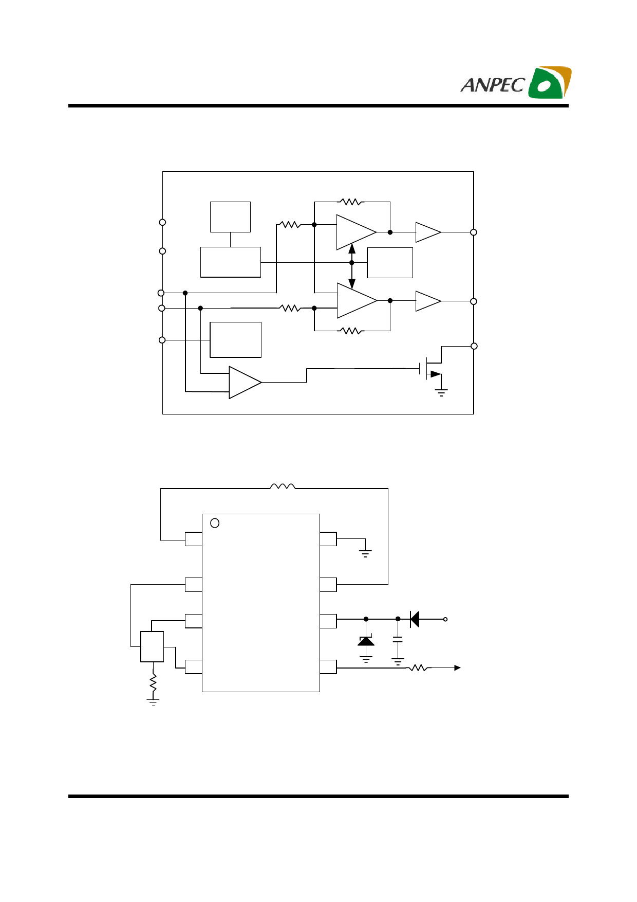
Block Diagram
VCC
GND
IN+
IN -
HB
OSC
Lock
Detection
Hall
Bias
_
+
500Ω
500Ω
150kΩ
-
+
TSD
+
-
150kΩ
OUT1
OUT2
FG
Typical Application Circuit
OUT2
1
IN+
2
HB
3
Hall
IN-
4
R1
GND
8
OUT1
7
D2
D1
VCC Zener
6
6V
FG
5
C1
RFG = 10kΩ
VIN
Pull High
Voltage
Note 3: In hot plug application, it’s necessary to protect against a hot plug input voltage overshoot by adding an input
zener diode between the VCC and GND to clamp the overshoot. In normal operation, the zener diode isn’t
stressed because output current doesn’t reverse to VCC.
Copyright © ANPEC Electronics Corp.
7
Rev. A.7 - Mar., 2008
www.anpec.com.tw
Share Link: 