RT9202CS 查看數據表(PDF) - Richtek Technology
零件编号
产品描述 (功能)
比赛名单
RT9202CS Datasheet PDF : 16 Pages
| |||
RT9202
Absolute Maximum Ratings
z Supply Voltage VCC
7V
z BOOT & UGATE to GND
15V
z Input, Output or I/O Voltage
GND−0.3V ~ 7V
z Power Dissipation, PD @ TA = 25°C
SOP-8
0.625W
z Package Thermal Resistance
SOP-8, θJA
z Ambient Temperature Range
160°C/W
0°C ~ +70°C
z Junction Temperature Range
-40°C ~ +125°C
z Storage Temperature Range
-65°C ~ +150°C
z Lead Temperature (Soldering, 10 sec.)
260°C
CAUTION:
Stresses beyond the ratings specified in “Absolute Maximum Ratings” may cause permanent damage to the
device. This is a stress only rating and operation of the device at these or any other conditions above those
indicated in the operational sections of this specification is not implied.
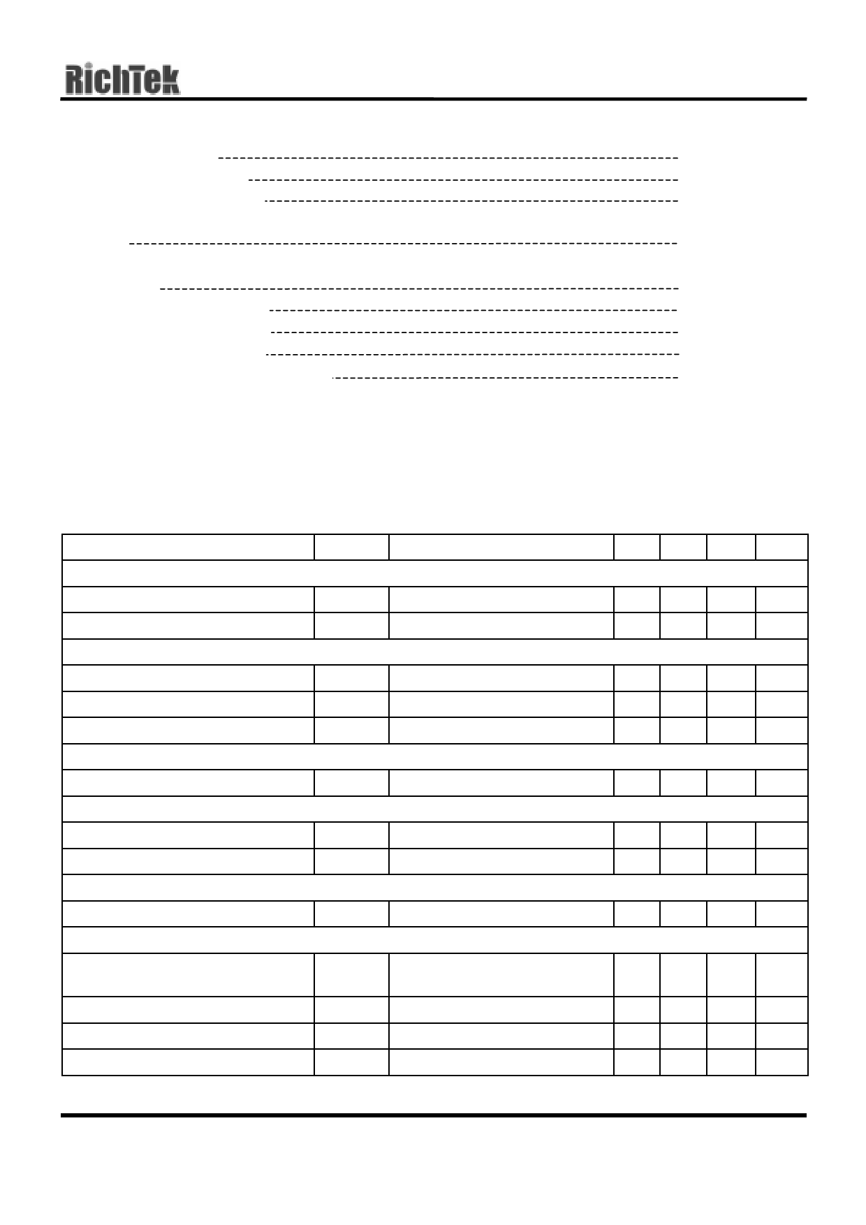
Electrical Characteristics
(VCC = 5V, TA = 25°C, Unless otherwise specified.)
Parameter
Symbol
Test Conditions
VCC Supply Current / Regulated Voltage
Nominal Supply Current
Regulated Voltage from BOOT
Power-On Reset
ICC
UGATE, LGATE open
VCC
VBOOT = 12V
Rising VCC Threshold
VCC Threshold Hysteresis
Rising VOCSET Threshold
Reference
VOCSET = 4.5V
VOCSET1 = 4.5V
Reference Voltage
Oscillator
Free Running Frequency
Ramp Amplitude
Error Amplifier
∆ VOSC
DC gain
PWM Controller Gate Driver
Upper Drive Source
Upper Drive Sink
Lower Drive Source
Lower Drive Sink
RUGATE
RUGATE
RLGATE
RLGATE
BOOT= 12V
BOOT-VUGATE = 1V
VUGATE = 1V
VCC - VLGATE = 1V,
VLGATE = 1V
Min Typ Max Units
--
3
6 mA
5
6
7
V
3.85 4.1 4.35 V
0.3 0.5 0.7 V
0.8 1.25 2.0 V
0.784 0.8 0.816 V
250 300 350 KHz
-- 1.75 -- VP-P
32 35 38 dB
--
7
11
Ω
--
5 7.5
Ω
--
4
6
Ω
--
2
4
Ω
To be continued
DS9202-02 August 2002
www.richtek.com
5
Share Link: 