RT9161 查看數據表(PDF) - Richtek Technology
零件编号
产品描述 (功能)
比赛名单
RT9161 Datasheet PDF : 12 Pages
| |||
RT9161/A
Absolute Maximum Ratings
• Input Voltage
• Operating Junction Temperature Range
• Storage Temperature Range
• Power Dissipation, PD @ TA = 25°C
SOT-89
TO-92
SOT-23
• Package Thermal Resistance
SOT-89, θJC
SOT-89, θJA
SOT-223, θJC
SOT-223, θJA
TO-92, θJA
SOT-23, θJA
-0.3 ~ 14V
-40°C ~ 125°C
-65°C ~ 150°C
0.5W
0.6W
0.15W
100°C /W
300°C/W
15°C/W
60°C/W
160°C/W
250°C/W
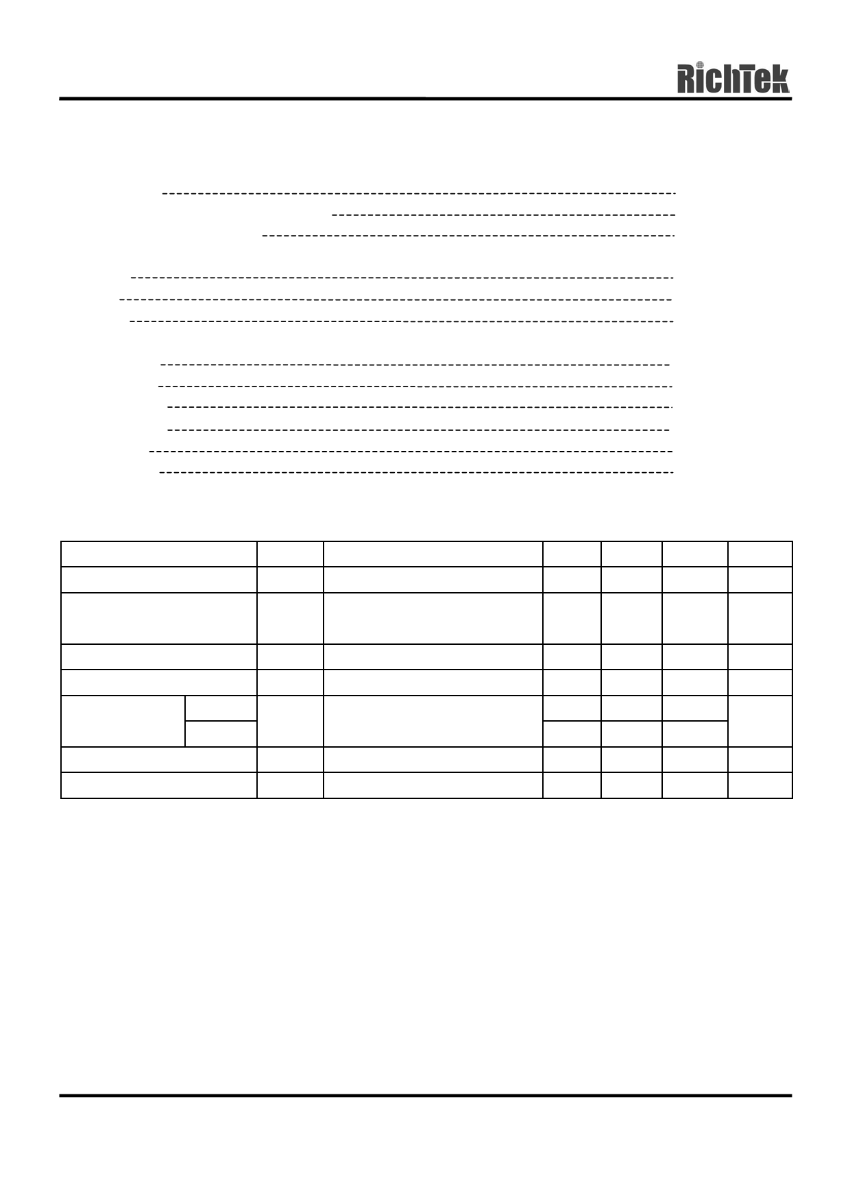
Electrical Characteristics
(TA = 25°C, CIN = 1µF, COUT = 10µF, unless otherwise specified.)
Parameter
Symbol
Test Conditions
Output Voltage Accuracy
∆VOUT IL = 1mA, VIN = 5V
Output Voltage Temperature
Coefficient
Min
Typ
Max Units
-2
--
+2
%
--
50
150 PPM/°C
Line Regulation
∆VLINE IL = 1mA, VIN = 4.5 ~ 12V
--
Load Regulation (2)
∆VLOAD IL = 1mA ~ 300/500mA, VIN = 5V --
RT9161
350
Current Limit (3)
ILIMIT
VIN = 5V, VOUT = 0V
RT9161A
500
2
3
%VOUT
1
30/50 mV
580
--
mA
900
--
Dropout Voltage (4) (5)
VDROP IL = 300/500mA
-- 450/750 600/1000 mV
Standby Current
ISTANDBY IL = 0, VIN = 12V
--
110
180
µA
Note:
(1) Guaranteed by design.
(2) Regulation is measured at constant junction temperature, using pulsed ON time.
(3) Current Limit is measured at constant junction temperature, using pulsed ON time.
(4) Dropout is measured at constant junction temperature, using pulsed ON time, and the criterion is VOUT inside
target value ± 2%.
(5) Dropout test is skipped at the condition of VIN < 3V.
www.richtek.com
2
DS9161/A-20 November 2002
Share Link: 