CM75DY-34A 查看數據表(PDF) - Mitsumi
零件编号
产品描述 (功能)
比赛名单
CM75DY-34A Datasheet PDF : 8 Pages
| |||
< IGBT MODULES >
CM75DY-34A
HIGH POWER SWITCHING USE
INSULATED TYPE
Note1. Represent ratings and characteristics of the anti-parallel, emitter-collector free wheeling diode (FWDi).
2. Case temperature (TC) and heat sink temperature (T s ) are defined on the each surface (mounting side) of base plate and heat sink just under
the chips. Refer to the figure of chip location.
The heat sink thermal resistance should measure just under the chips.
3. Pulse width and repetition rate should be such that the device junction temperature (T j ) dose not exceed T j m a x rating.
4. Junction temperature (T j ) should not increase beyond T j m a x rating.
5. Pulse width and repetition rate should be such as to cause negligible temperature rise. Refer to the figure of test circuit.
6. Typical value is measured by using thermally conductive grease of λ=0.9 W/(m·K).
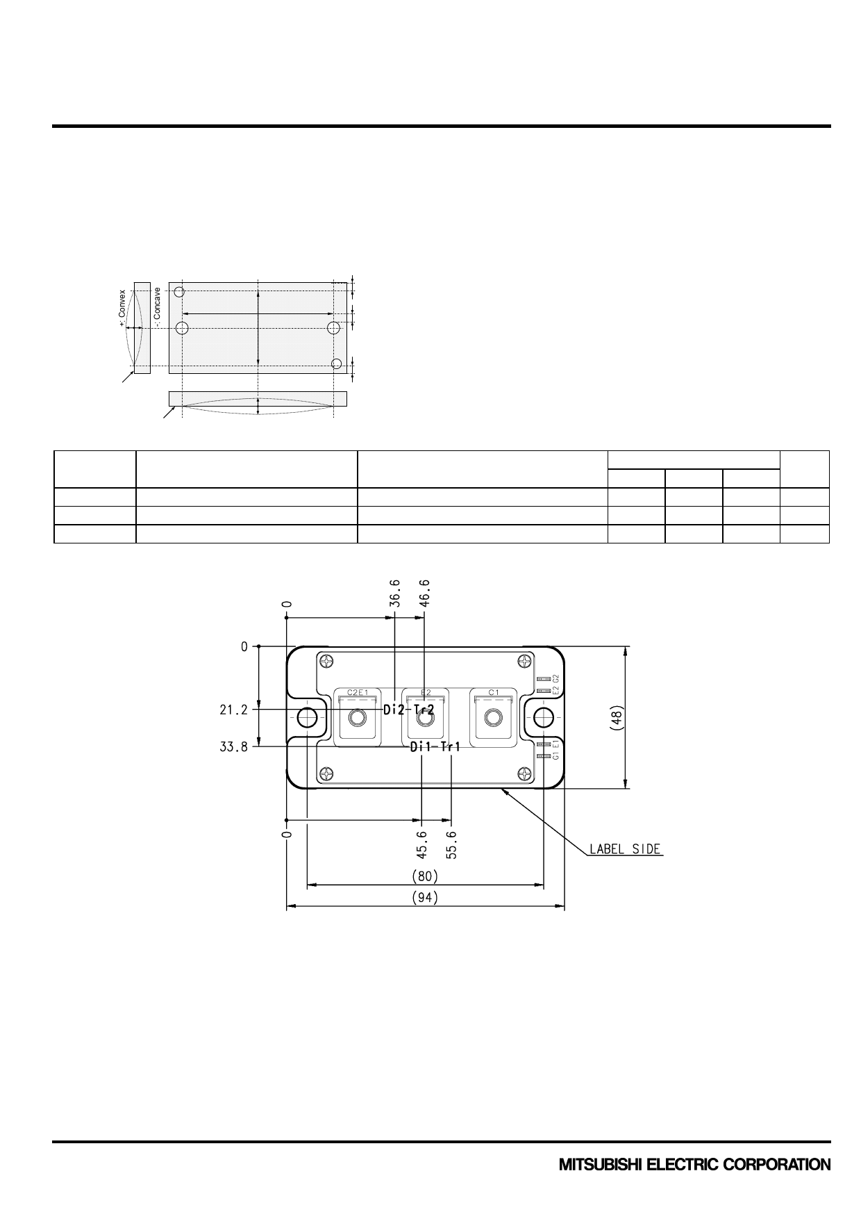
7. Base plate (mounting side) flatness measurement points (X, Y) are as follows of the following figure.
3 mm
X
3 mm
Mounting
side
Y
Mounting side
-: Concave
3 mm
Mounting side
+: Convex
RECOMMENDED OPERATING CONDITIONS
Symbol
Item
VCC
VGEon
RG
(DC) Supply voltage
Gate (-emitter drive) voltage
External gate resistance
CHIP LOCATION (Top view)
Conditions
Applied across C1-E2
Applied across G1-Es1/G2-Es2
Per switch
Limits
Unit
Min.
Typ.
Max.
-
1000
1100
V
13.5
15.0
16.5
V
6.4
-
64
Ω
Dimension in mm, tolerance: ±1 mm
Tr1/Tr2: IGBT, Di1/Di2: FWDi
Publication Date : June.2011
3
Share Link: 