RF2619PCBA 查看數據表(PDF) - RF Micro Devices
零件编号
产品描述 (功能)
比赛名单
RF2619PCBA Datasheet PDF : 8 Pages
| |||
RF2619
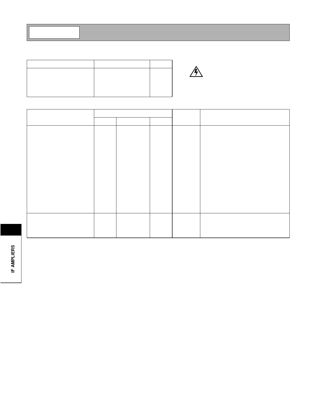
Absolute Maximum Ratings
Parameter
Supply Voltage
Control Voltage
Input Power Levels
Operating Ambient Temperature
Storage Temperature
Rating
-0.5 to +7.0
-0.5 to +5.0
+10
-40 to +85
-40 to +150
Unit
VDC
V
dBm
°C
°C
Caution! ESD sensitive device.
RF Micro Devices believes the furnished information is correct and accurate
at the time of this printing. However, RF Micro Devices reserves the right to
make changes to its products without notice. RF Micro Devices does not
assume responsibility for the use of the described product(s).
Parameter
Overall
10
Frequency Range
Maximum Gain
Minimum Gain
Gain Slope
Gain Control Voltage Range
Gain Control Input Impedance
Noise Figure
Input IP3
Input Impedance
Stability (Max VSWR)
Power Supply
Voltage
Current Consumption
Current Consumption
Specification
Min.
Typ.
Max.
12 to 175
+39
+42
-48
-45
57
0 to 3
30
10.5
13
-26
-25
1
10:1
2.7 to 3.3
23
25
22
24
Unit
MHz
dB
dB
dB/V
VDC
kΩ
dB
dBm
kΩ
Condition
T=25°C, 130MHz, VCC=3.0V, Pin=-
40dBm, ZS=1kΩ, ZL=1kΩ, 1kΩ External
Output Terminating Resistor (Effective
ZL=500Ω) (See Application Example)
VGC =2.4 V
VGC = 0.3 V
Measured in 0.5V increments
At maximum gain and 130MHz
At +10 gain and referenced to 1kΩ,
Pin=-45dBm per tone
Differential
Spurious < -70 dBm
V
mA
Maximum gain, VCC=3.0V
mA
Minimum gain, VCC=3.0V
10-26
Rev B5 010720
Share Link: 