LIS331DLTR(2007) 查看數據表(PDF) - STMicroelectronics
零件编号
产品描述 (功能)
比赛名单
LIS331DLTR
(Rev.:2007)
(Rev.:2007)
STMicroelectronics

LIS331DLTR Datasheet PDF : 38 Pages
| |||
LIS331DL
Mechanical and electrical specifications
2.3
Communication interface characteristics
2.3.1
SPI interface
Subject to general operating conditions for Vdd and Top.
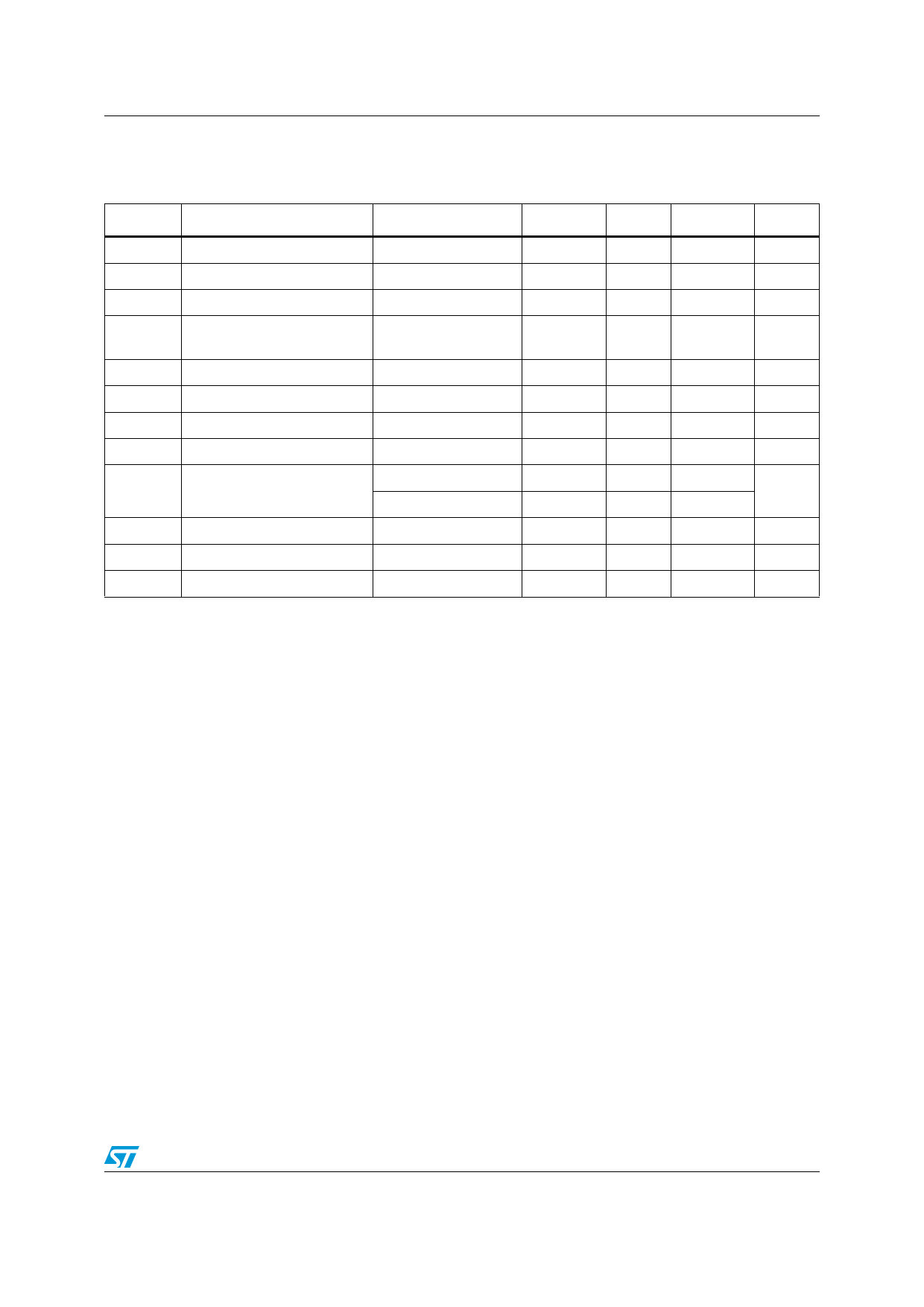
Table 4. SPI slave timing values
Symbol
Parameter
tc(SPC)
fc(SPC)
tsu(CS)
th(CS)
tsu(SI)
th(SI)
tv(SO)
th(SO)
tdis(SO)
SPI clock cycle
SPI clock frequency
CS setup time
CS hold time
SDI input setup time
SDI input hold time
SDO valid output time
SDO output hold time
SDO output disable time
Value Note: 1
Min
Max
100
10
5
8
5
15
50
6
50
Unit
ns
MHz
ns
Figure 4. SPI slave timing diagram (2)
CS (3)
SPC (3)
tsu(CS)
SDI (3)
SDO (3)
tc(SPC)
tsu(SI)
th(SI)
MSB IN
tv(SO)
MSB OUT
th(SO)
(3)
th(CS)
(3)
LSB IN
(3)
tdis(SO)
LSB OUT
(3)
Note: 1 Values are guaranteed at 10MHz clock frequency for SPI with both 4 and 3 wires, based on
characterization results, not tested in production
2 Measurement points are done at 0.2·Vdd_IO and 0.8·Vdd_IO, for both Input and output
ports
3 When no communication is on-going, data on CS, SPC, SDI and SDO are driven by internal
pull-up resistors
11/38
Share Link: