LT3464 查看數據表(PDF) - Linear Technology
零件编号
产品描述 (功能)
比赛名单
LT3464 Datasheet PDF : 16 Pages
| |||
LT3464
APPLICATIO S I FOR ATIO
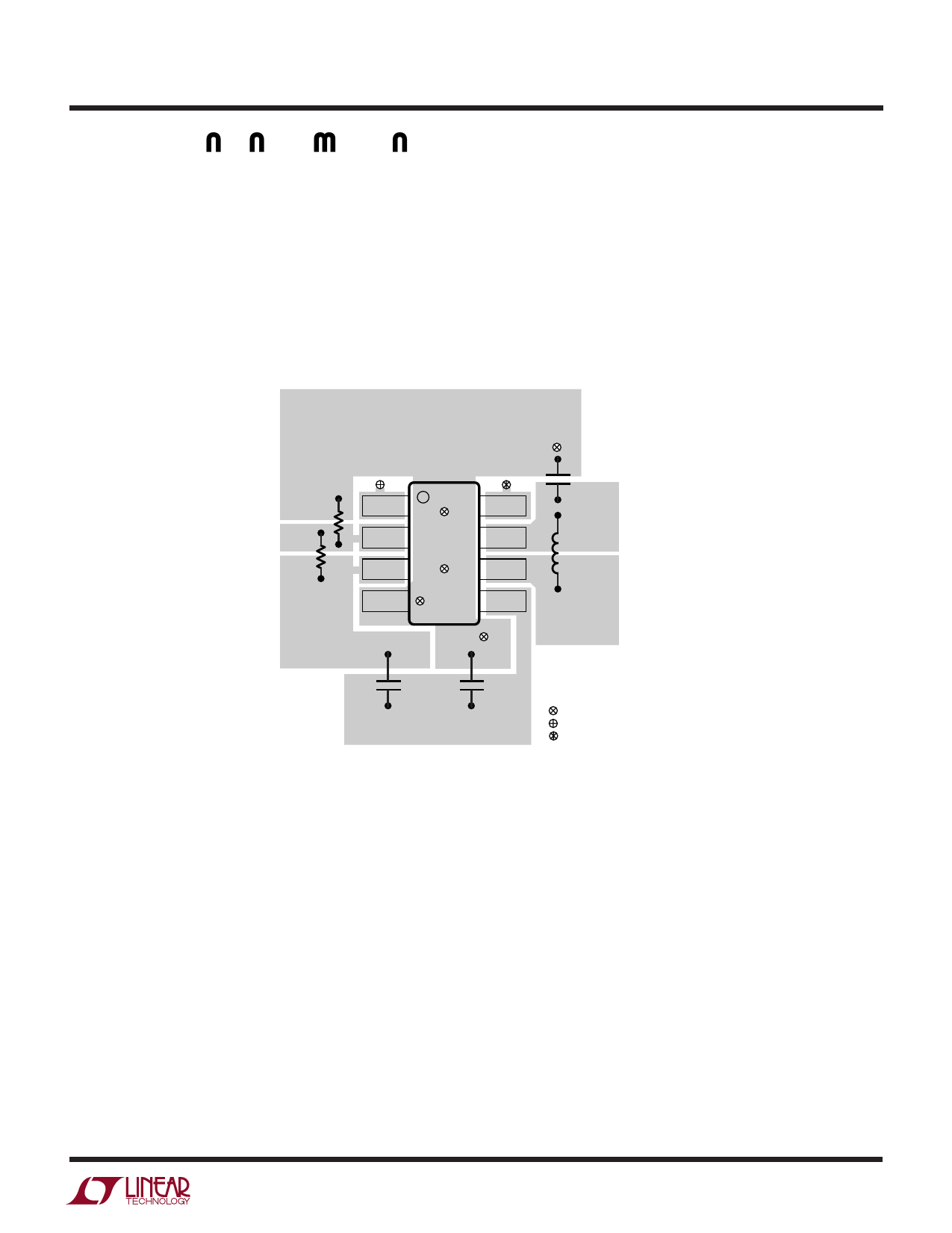
Board Layout Considerations
As with all switching regulators, careful attention must be
paid to the PCB board layout and component placement.
To maximize efficiency, switch rise and fall times are made
as short as possible. To prevent electromagnetic interfer-
ence (EMI) problems, proper layout of the high frequency
switching path is essential. The voltage signal of the SW
pin has sharp rising and falling edges. Minimize the length
and area of all traces connected to the SW pin and always
use a ground plane under the switching regulator to
minimize interplane coupling. In addition, the ground
connection for the feedback resistor R1 should be tied
directly to the GND pin and not shared with any other
component, ensuring a clean, noise-free connection. Rec-
ommended component placement is shown in Figure 6.
GND
VIN
GND
VOUT
3464 F07
VIAS TO GROUND PLANE
VIA TO CONTROL
VIA TO SHDN
Figure 6. Recommended Layout
3464f
11
Share Link: 