TDA9861 查看數據表(PDF) - Philips Electronics
零件编号
产品描述 (功能)
比赛名单
TDA9861 Datasheet PDF : 18 Pages
| |||
Philips Semiconductors
Universal HiFi audio processor for TV
Preliminary specification
TDA9861
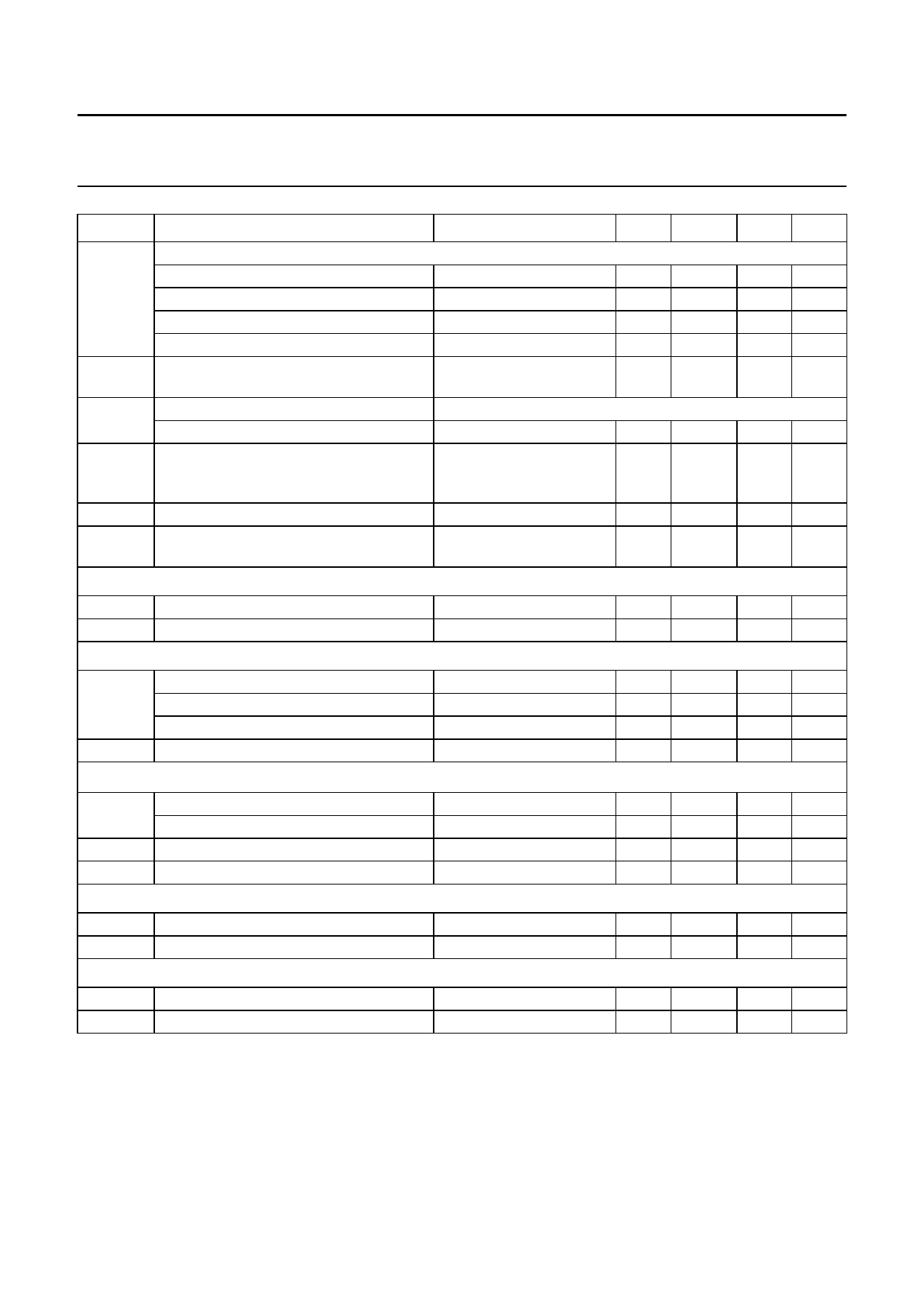
SYMBOL
PARAMETER
CONDITIONS
VN(W)
weighted noise voltage at output (quasi-peak level) CCIR468-3
for +16 dB gain
for 0 dB gain
for −16 dB gain
for mute position
B
AF bandwidth
Gv = −80 dB
−1 dB
THD
total harmonic distortion
f = 20 to 12500 Hz
αsp
αbus
RR100
for Vi = 1 V (RMS value)
stereo channel separation
crosstalk of I2C-bus
ripple rejection with 100 Hz ripple on VP
Gv = −40 to 0 dB
f = 10 kHz; Gv = 0 dB;
opposite input grounded
by 1 kΩ resistor
Gv = 0 dB; note 1
Gv = 0 dB;
VR < 200 mV RMS
SCART output (pins 7 and 26)
Vo
maximum output signal (RMS value)
THD ≤ 0.5%; RL > 5 kΩ
RL
admissible output load resistor
Power on reset
VPONR
increasing supply voltage
start of reset
end of reset
VPONR decreasing supply voltage start of reset
I2C-bus, SCL and SDA (pins 16 and 17, observe I2C-bus specification)
V16, 17
input voltage HIGH-level
input voltage LOW-level
I16, 17
VACK
input current
output voltage at acknowledge (pin 17)
I17 = −3 mA
Module address (pin 25)
VIL
LOW level input voltage
VIH
HIGH level output voltage
Port outputs P1 and P2 (open-collector outputs pins 2 and 31)
VOL
I2, 31
LOW level output voltage
port output current
I2, 31 = 1 mA (sink)
sink current
Note to the characteristics
1. αbus = 20 log Vbus / Vo (Vbus = spurious bus signal voltage on AF output pin).
MIN. TYP.
−
115
−
20
−
15
−
12
−
20 to
20000
−
0.08
−
75
−
100
−
55
2
−
5
−
−
−
5.2 6.0
4.4 5.2
3
−
0
−
−
−
−
−
0
−
3
−
−
−
−
−
MAX. UNIT
−
µV
−
µV
−
µV
−
µV
−
Hz
0.25 %
−
dB
−
dB
−
dB
−
V
−
kΩ
2.5 V
6.8 V
6.0 V
VP
V
1.5 V
±10 µA
0.4 V
1.5 V
VP
V
0.3 V
1
mA
June 1994
9
Share Link: 