SAF-XC858CA-16FFI5V 查看數據表(PDF) - Infineon Technologies
零件编号
产品描述 (功能)
比赛名单
SAF-XC858CA-16FFI5V Datasheet PDF : 124 Pages
| |||
XC858CA
Functional Description
3
Functional Description
Chapter 3 provides an overview of the XC858 functional description.
3.1
Processor Architecture
The XC858 is based on a high-performance 8-bit Central Processing Unit (CPU) that is
compatible with the standard 8051 processor. While the standard 8051 processor is
designed around a 12-clock machine cycle, the XC858 CPU uses a 2-clock machine
cycle. This allows fast access to ROM or RAM memories without wait state. The
instruction set consists of 45% one-byte, 41% two-byte and 14% three-byte instructions.
The XC858 CPU provides a range of debugging features, including basic stop/start,
single-step execution, breakpoint support and read/write access to the data memory,
program memory and Special Function Registers (SFRs).
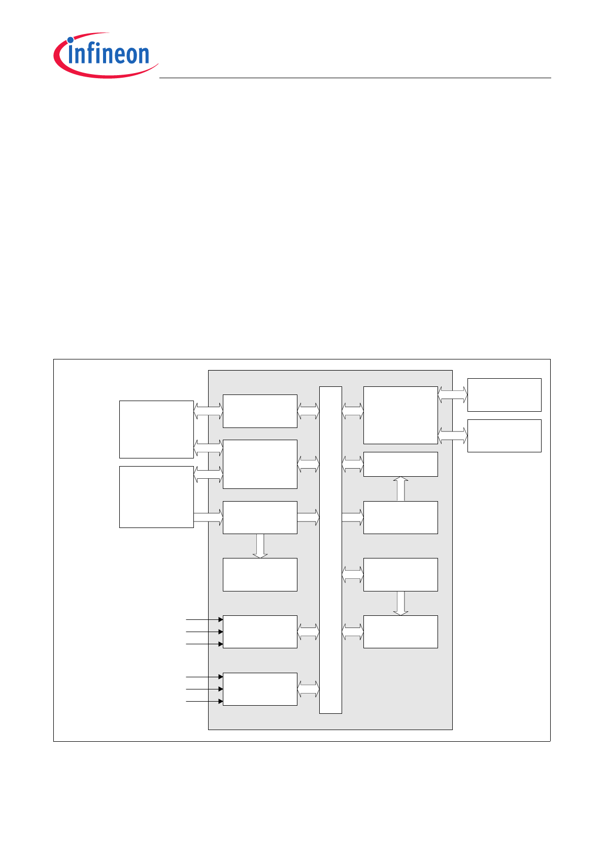
Figure 5 shows the CPU functional blocks.
External Data
Memory
Program Memory
fCCLK
Memory Wait
Reset
Legacy External Interrupts (IEN0, IEN1)
External Interrupts
Non-Maskable Interrupt
Core SFRs
16-bit Registers &
Memory Interface
Opcode &
Immediate
Registers
Opcode Decoder
State Machine &
Power Saving
Interrupt
Controller
Register Interface
ALU
Internal Data
Memory
External SFRs
Multiplier / Divider
Timer 0 / Timer 1
UART
Figure 5 CPU Block Diagram
Data Sheet
16
V1.0, 2010-03
Share Link: 