TD62604PG 查看數據表(PDF) - Toshiba
零件编号
产品描述 (功能)
比赛名单
TD62604PG Datasheet PDF : 8 Pages
| |||
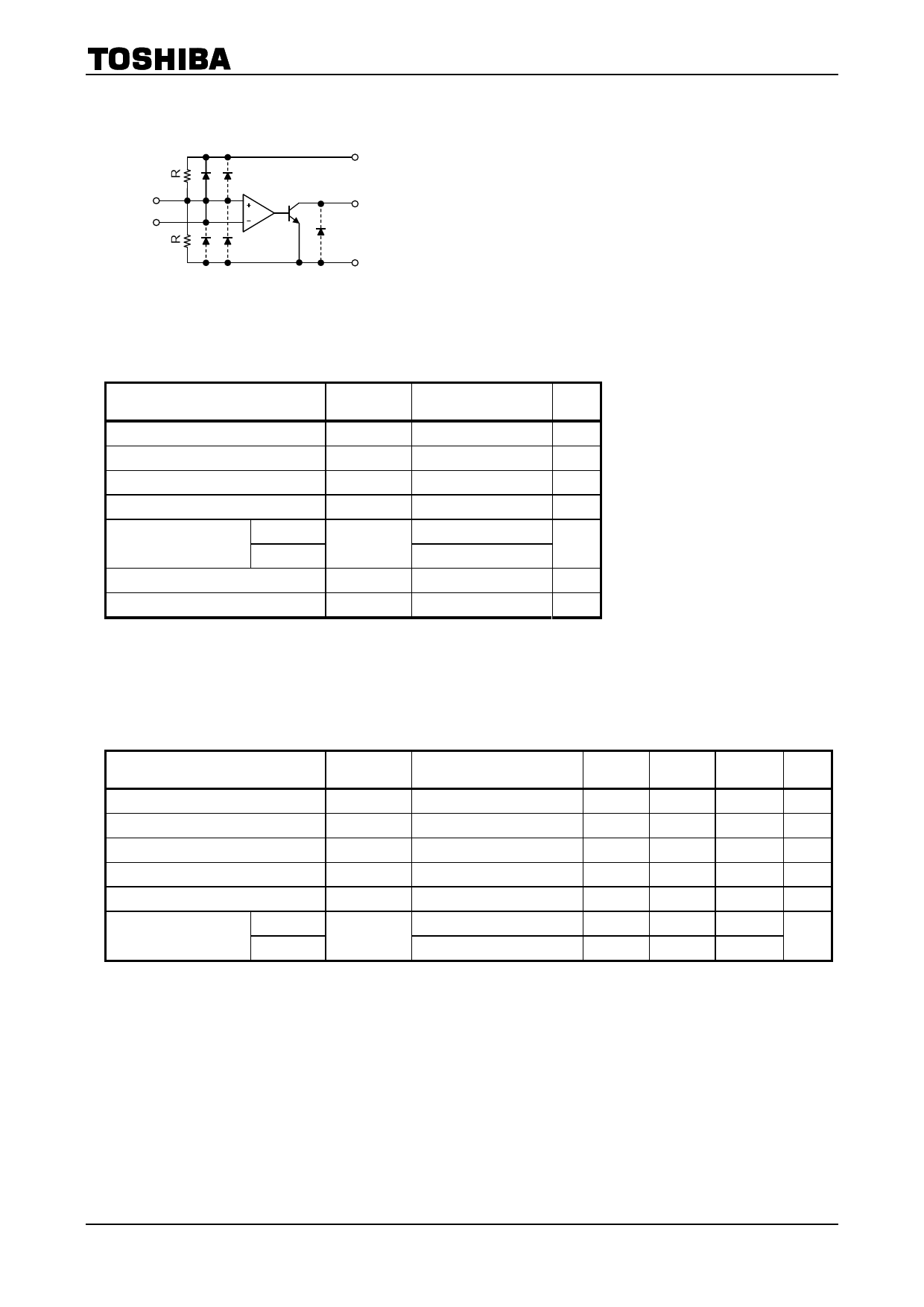
Schematics (each driver)
TD62604PG/FG
Vref
INPUT
VCC
OUTPUT
GND
Note: The output parasitic diodes cannot be used as clamp diodes.
Absolute Maximum Ratings (Ta = 25°C)
Characteristics
Symbol
Rating
Unit
Supply voltage
Output sustaining voltage
Output current
Input voltage
PG
Power dissipation
FG
Operating temperature
Storage temperature
VCC
VOUT
IOUT
VIN
PD (Note 2)
Topr
Tstg
20
V
−0.5 to 20
V
10
mA/ch
−0.5 to VCC + 0.5
V
1.0
W
0.625 (Note 1)
−40 to 85
°C
−55 to 150
°C
Note 1: On PCB (30 × 30 × 1.6 mm Cu 50%)
Note 2: Derated above 25°C in the proportion of 8.0 mW/°C (PG type), 5.0 mW/°C (FG type).
Operating Ranges (Ta = −40 to 85°C)
Characteristics
Supply voltage
Output sustaining voltage
Output current
Input voltage
REF, input voltage
PG
Power dissipation
FG
Symbol
VCC
VOUT
IOUT
VIN
Vref
PD
Condition
⎯
⎯
VCC = 5 V
⎯
Ta = 25°C
⎯
On PCB
Min
Typ.
Max
Unit
4.0
⎯
18
V
0
⎯
18
V
0
⎯
8
mA/ch
0
⎯
VCC
V
0.4
⎯
VCC - 1.6 V
⎯
⎯
0.36
W
⎯
⎯
0.325
2
2009-11-24
Share Link: 