PCK2010RDL 查看數據表(PDF) - Philips Electronics
零件编号
产品描述 (功能)
比赛名单
PCK2010RDL Datasheet PDF : 18 Pages
| |||
Philips Semiconductors
CK98R (100/133MHz) RCC spread spectrum
system clock generator
Product specification
PCK2010R
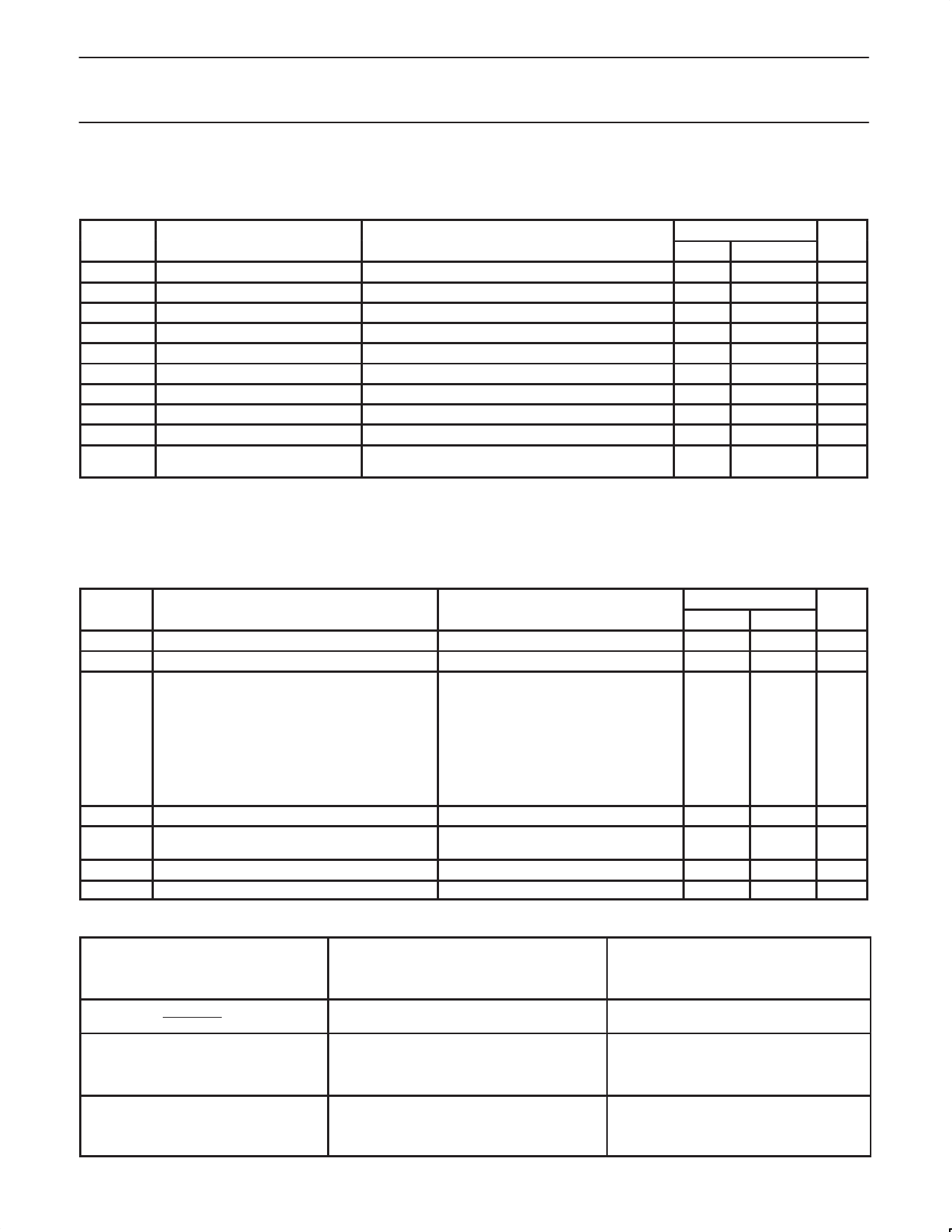
ABSOLUTE MAXIMUM RATINGS1, 2
In accordance with the Absolute Maximum Rating System (IEC 134)
Voltages are referenced to VSS (VSS = 0 V)
SYMBOL
PARAMETER
CONDITION
LIMITS
MIN
MAX
UNIT
VDD3
DC 3.3 V core supply voltage
–0.5
+4.6
V
VDDQ3 DC 3.3 V I/O supply voltage
–0.5
+4.6
V
VDDQ2 DC 2.5 V I/O supply voltage
–0.5
+3.6
V
IIK
DC input diode current
VI < 0
–50
mA
VI
DC input voltage
Note 2
–0.5
5.5
V
IOK
DC output diode current
VO > VCC or VO < 0
±50
mA
VO
DC output voltage
Note 2
–0.5
VCC + 0.5
V
IO
DC output source or sink current
VO = 0 to VCC
±50
mA
TSTG
Storage temperature range
–65
+150
°C
PTOT
Power dissipation per package
plastic medium-shrink (SSOP)
For temperature range: –40 to +125°C
above +55°C derate linearly with 11.3mW/K
850
mW
NOTES:
1. Stresses beyond those listed may cause permanent damage to the device. These are stress ratings only and functional operation of the
device at these or any other conditions beyond those indicated under “recommended operating conditions” is not implied. Exposure to
absolute-maximum-rated conditions for extended periods may affect device reliability.
2. The input and output voltage ratings may be exceeded if the input and output current ratings are observed.
RECOMMENDED OPERATING CONDITIONS
SYMBOL
PARAMETER
VDD3V
VDD25V
CL
VI
VO
fREF
Tamb
DC 3.3 V core supply voltage
DC 2.5 V I/O supply voltage
Capacitive load on:
CPUCLK
PCICLK
CPUDIV2
3V66
48 MHz clock USB
REF
IOAPIC
DC input voltage range
DC output voltage range
Reference frequency, oscillator nominal value
Operating ambient temperature range in free air
CONDITIONS
1 device load, possible 2 loads
Must meet PCI 2.1 requirements
1 device load, possible 2 loads
1 device load, possible 2 loads
1 device load
1 device load
1 device load
LIMITS
MIN
MAX
3.135
3.465
2.375
2.625
UNIT
V
V
10
10
10
10
10
10
10
0
0
14.31818
0
20
30
20
30
20
20
20
VDD3V
VDD25V
VDD3V
14.31818
+70
pF
pF
pF
pF
pF
pF
pF
V
V
MHz
°C
POWER MANAGEMENT
CK133
CONDITION
Power-down mode
(PWRDWN = 0)
Full active 100 MHz
SEL133/100# = 0
SEL1, 0 = 1 1
CPUSTOP, PCISTOP = 1
Full active 133 MHz
SEL133/100# = 1
SEL1, 0 = 1 1
CPUSTOP, PCISTOP = 1
MAXIMUM 2.5V SUPPLY CONSUMPTION
MAXIMUM DISCRETE CAP LOADS,
VDD25V = 2.625 V
ALL STATIC INPUTS = VDD3V OR VSS
100 µA
MAXIMUM 3.3V SUPPLY CONSUMPTION
MAXIMUM DISCRETE CAP LOADS,
VDD25V= 3.465 V
ALL STATIC INPUTS = VDD3V OR VSS
200 µA
80 mA
160 mA
90 mA
160 mA
1999 Oct 19
6
Share Link: 