IDT6198S20 查看數據表(PDF) - Integrated Device Technology
零件编号
产品描述 (功能)
比赛名单
IDT6198S20 Datasheet PDF : 8 Pages
| |||
IDT6198S/L
CMOS STATIC RAM 64K (16K x 4-BIT)
MILITARY AND COMMERCIAL TEMPERATURE RANGES
AC ELECTRICAL CHARACTERISTICS (VCC = 5.0V ± 10%, All Temperature Ranges)
6198S15(1)
6198L15(1)
6198S20
6198L20
6198S25
6198L25
6198S35 6198S45/55(2) 6198S70/85(2)
6198L35 6198L45/55(2) 6198L70/85(2)
Symbol
Parameter
Min. Max. Min. Max. Min. Max. Min. Max. Min. Max. Min. Max. Unit
Read Cycle
tRC
Read Cycle Time
15 — 20 — 25 — 35 — 45/55 — 70/85 — ns
tAA
Address Access Time
— 15 — 19 — 25 — 35 — 45/55 — 70/85 ns
tACS Chip Select Access Time
tCLZ(3) Chip Select to Output in Low-Z
— 15 — 20 —
5 — 5 —5
25 — 35 — 45/55 — 70/85 ns
— 5 — 5 — 5 — ns
tOE
tOLZ(3)
tCHZ(3)
tOHZ(3)
Output Enable to Output Valid
Output Enable to Output in Low-Z
Chip Select to Output in High-Z
Output Disable to Output in High-Z
— 8 — 9—
5 — 5 —5
2 7 2 82
2 7 2 82
11 — 18 — 25/35 — 45/55 ns
— 5 — 5 — 5 — ns
10 2 14 — 15/20 — 25/30 ns
9 2 15 — 15/20 — 25/30 ns
tOH
Output Hold from Address Change
5 — 5 —2
tPU(3) Chip Select to Power Up Time
0 — 0 —0
tPD(3) Chip Deselect to Power Down Time — 15 — 20 —
NOTES:
1. 0° to +70°C temperature range only.
2. –55°C to +125°C temperature range only.
3. This parameter is guaranteed by device characterization but is not production tested.
— 5 — 5 — 5 — ns
— 0 — 0 — 0 — ns
25 — 35 — 45/55 — 70/85 ns
2987 tbl 11
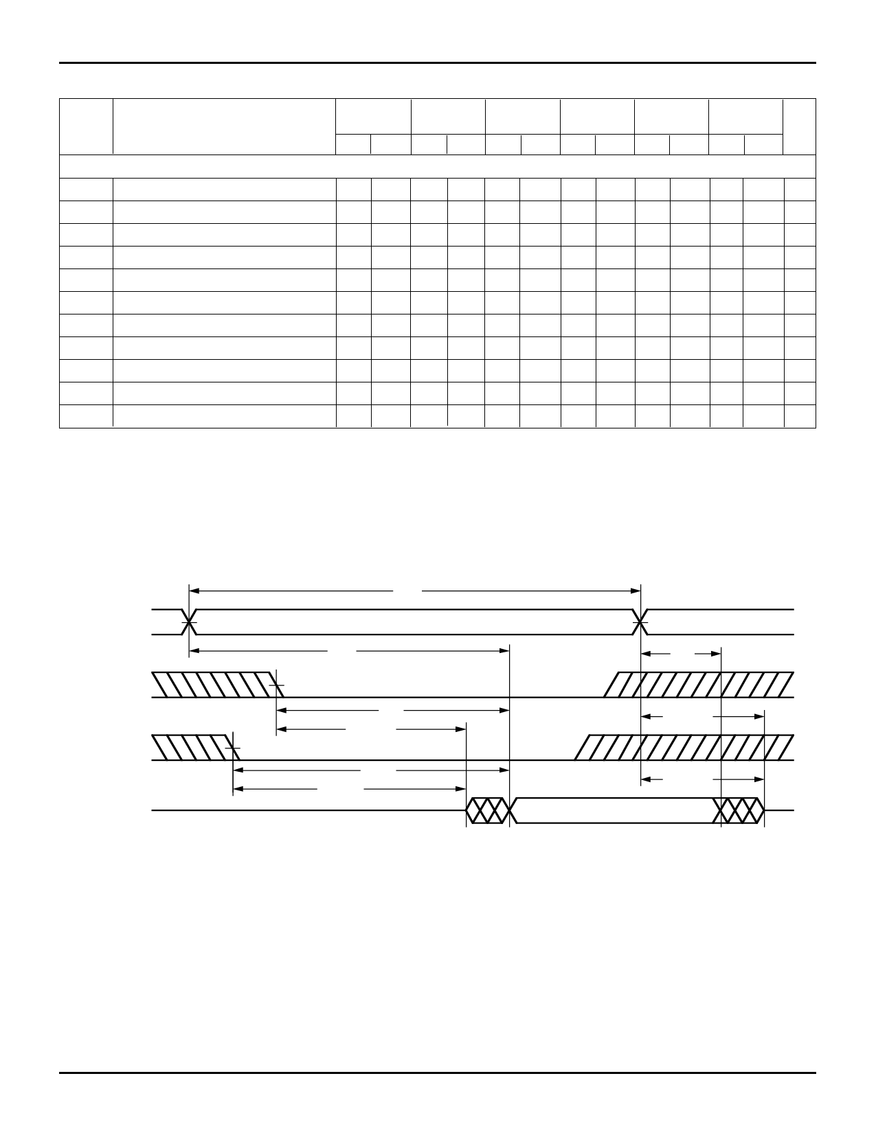
TIMING WAVEFORM OF READ CYCLE NO. 1(1)
tRC
ADDRESS
OE
CS
DATAOUT
tAA
tOE
tOLZ (5)
tACS
tCLZ (5)
NOTES:
1. WE is HIGH for Read cycle.
2. Device is continuously selected, CS is LOW.
3. Address valid prior to or coincident with CS transition LOW.
4. OE is LOW.
5. Transition is measured ±200mV from steady state voltage.
tOH
tOHZ (5)
tCHZ (5)
DATA VALID
2987 drw 07
6.3
5
Share Link: 