W921C880 查看數據表(PDF) - Winbond
零件编号
产品描述 (功能)
比赛名单
W921C880 Datasheet PDF : 57 Pages
| |||
W921E880A/W921C880
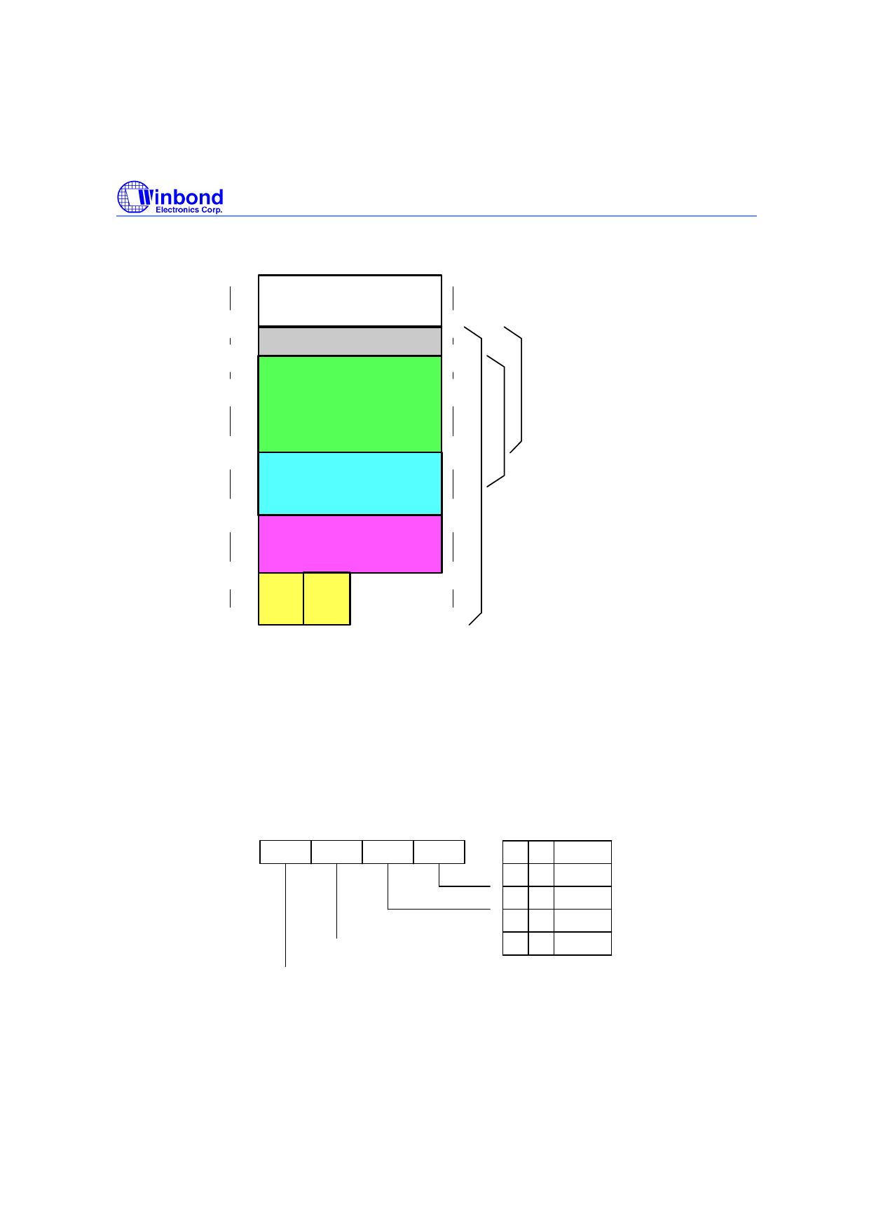
6.2 RAM Memory Map
000H
000
SPECIAL CONTROL REG.
03FH
040H
04FH
050H
063
064
WORKING REG.
079
080
07FH
SERIAL CONTROL REG. 127
080H
128
STACK REG.
STACK REG.
(40H - FFH)
OR GENERAL REG.
0FFH
255
100H
256
SERIAL CONTROL REG.
OR GENERAL REG.
17FH
383
SERIAL CONTROL REG.
(50H - 14EH)
180H
384
GENERAL REG.
GENERAL REG.
1FFH
511
200H
512
BANK0 BANK1
3FFH
1023
6.2.1 Special Control Reg. Area
There are 64 reg. × 4 bits in the special control register area. All control registers such as the DTMF
Control Reg., System Clock Control Reg. ...etc. are in this area. Please refer to the Spesial Control
Reg. Format.
Bank Select Reg.
BKSR REG: (ADDRESS = 001H)
(Default data = 0H)
b3
b2
b1
b0
Reserved
Reserved
b1 b0 BANK NO.
00
0
01
1
1 0 Reserved
1 1 Reserved
The Bank Select Reg. can select the active bank. The memory size of each bank is 512*4 bits. Bank 0 and bank 1 are normal
SRAM.
- 11 -
Publication Release Date: July 1999
Revision A3
Share Link: 