NCP1217(2004) 查看數據表(PDF) - ON Semiconductor
零件编号
产品描述 (功能)
比赛名单
NCP1217
(Rev.:2004)
(Rev.:2004)
ON Semiconductor

NCP1217 Datasheet PDF : 18 Pages
| |||
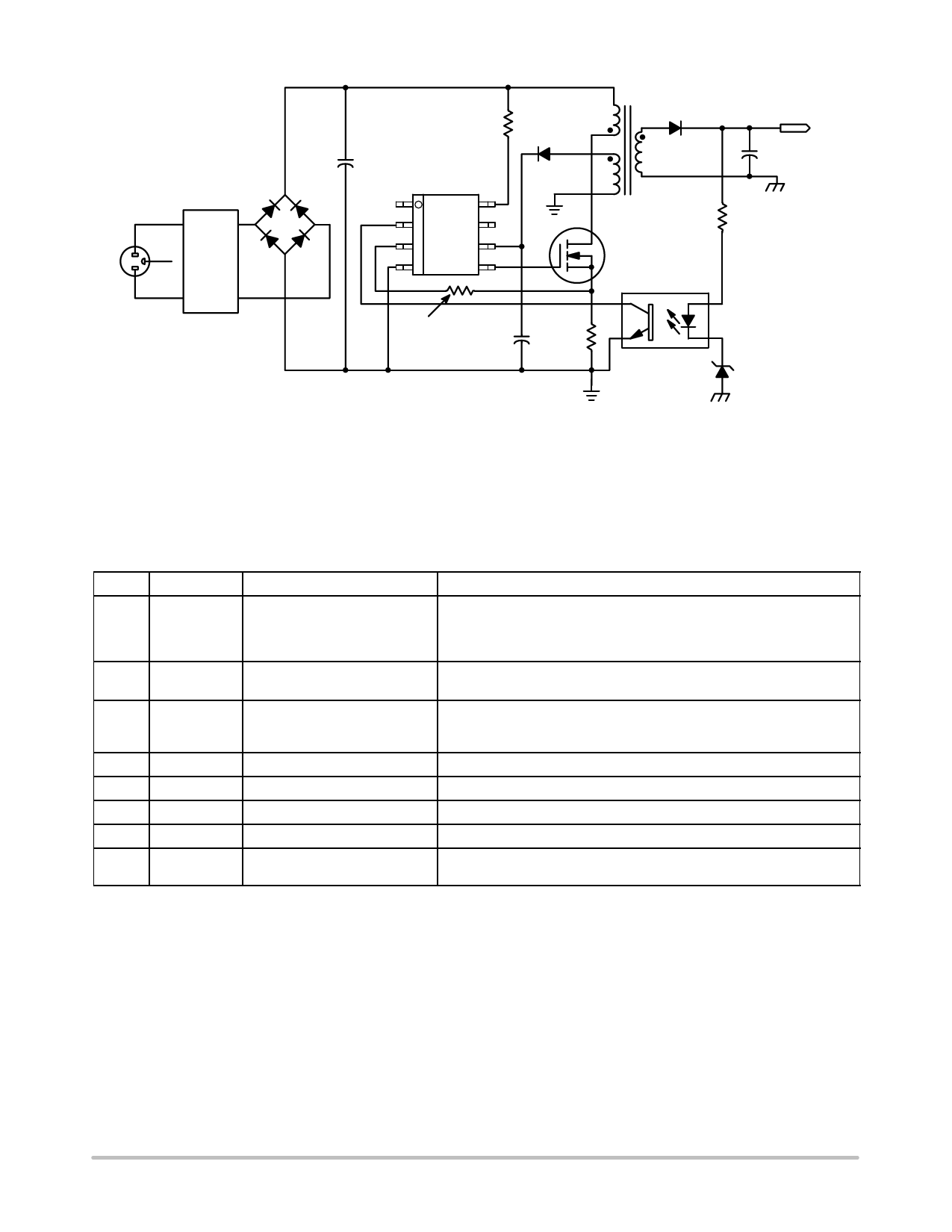
EMI
FILTER
UNIVERSAL
INPUT
NCP1217, NCP1217A
See Application
Section
+
NCP1217
Adj HV
1
8
2 FB
7
3 CS VCC 6
Gnd Drv
4
5
Aux.
Ramp Adjustment +
VOUT
+
Figure 1. Typical Application Example
ÁÁÁÁÁÁPPiInNÁÁÁNFoU.ÁÁÁNCTPÁÁÁIiOnNNÁÁÁaDmEÁÁÁeSCÁÁÁRIPÁÁÁTIOÁÁÁN ÁÁÁFunÁÁcÁtionÁÁÁÁÁÁÁÁÁÁÁÁÁÁÁÁÁÁÁÁÁÁÁÁÁÁÁÁÁÁÁÁÁDÁÁeÁscrÁÁÁiptioÁÁÁn ÁÁÁÁÁÁÁÁÁÁÁÁÁÁÁÁÁÁÁÁÁ
1
Adj
Adjust the skipping peak current This pin lets you adjust the level at which the cycle skipping process
takes place. Shorting this pin to ground permanently disables the skip
cycle feature.
By bringing this pin above 3.1 V, you permanently shut off the device.
2
FB
Sets the peak current setpoint By connecting an optocoupler to this pin, the peak current setpoint is
adjusted accordingly to the output power demand.
3
CS
Current sense input
This pin senses the primary current and routes it to the internal
comparator via an L.E.B. By inserting a resistor in series with the pin, you
control the amount of ramp compensation you need.
4
Gnd
The IC ground
−
5
Drv
Driving pulses
The driver’s output to an external MOSFET.
6
VCC
Supplies the IC
7
NC
−
This pin is connected to an external bulk capacitor of typically 22 mF.
This unconnected pin ensures adequate creepage distance.
8
HV
Ensures a clean and lossless
Connected to the high−voltage rail, this pin injects a constant current into
startup sequence
the VCC capacitor during the startup sequence.
http://onsemi.com
2
Share Link: