HEF4071BP 查看數據表(PDF) - NXP Semiconductors.
零件编号
产品描述 (功能)
比赛名单
HEF4071BP Datasheet PDF : 11 Pages
| |||
NXP Semiconductors
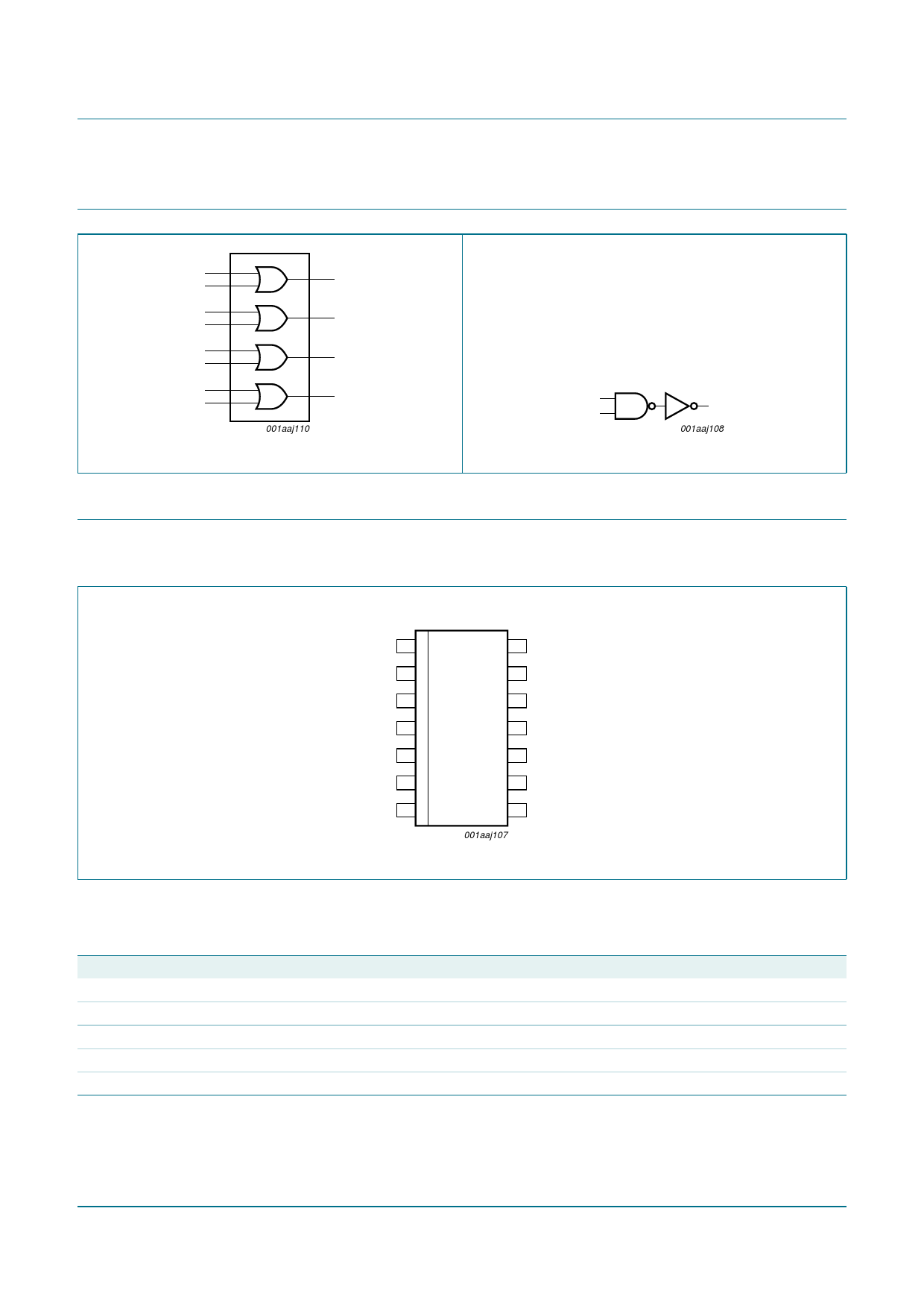
4. Functional diagram
HEF4071B
Quad 2-input OR gate
1 1A
2 1B
5 2A
6 2B
8 3A
9 3B
12 4A
13 4B
1Y 3
2Y 4
3Y 10
4Y 11
001aaj110
Fig 1. Functional diagram
5. Pinning information
5.1 Pinning
nA
nY
nB
001aaj108
Fig 2. Logic diagram (one gate)
Fig 3. Pin configuration
HEF4071B
1A 1
1B 2
1Y 3
2Y 4
2A 5
2B 6
VSS 7
14 VDD
13 4B
12 4A
11 4Y
10 3Y
9 3B
8 3A
001aaj107
5.2 Pin description
Table 2.
Symbol
1A to 4A
1B to 4B
1Y to 4Y
VSS
VDD
Pin description
Pin
1, 5, 8, 12
2, 6, 9, 13
3, 4, 10, 11
7
14
Description
input
input
output
ground (0 V)
supply voltage
HEF4071B_4
Product data sheet
Rev. 04 — 28 November 2008
© NXP B.V. 2008. All rights reserved.
2 of 11
Share Link: 