RT9264CS 查看數據表(PDF) - Unspecified
零件编号
产品描述 (功能)
比赛名单
RT9264CS Datasheet PDF : 8 Pages
| |||
Preliminary
RT9264
Pin Description
Pin No. Pin Name Pin Function
1 GND
Ground
2 EXT
Output pin for driving external NMOS or NPN
When driving an NPN, a resistor should be added for limiting base current.
3 LFB
Feedback pin of the built-in LDO (Internal Vref = 0.86V)
4
LDOO
Voltage output pin of the built-in LDO
5 FB
Feedback input pin
Internal reference voltage for the error amplifier is 1.25V.
6 VDD
7 LX
Input positive power pin of RT9264
Pin for switching
8 CE
Chip enable
RT9264 gets into shutdown mode when CE pin set to low.
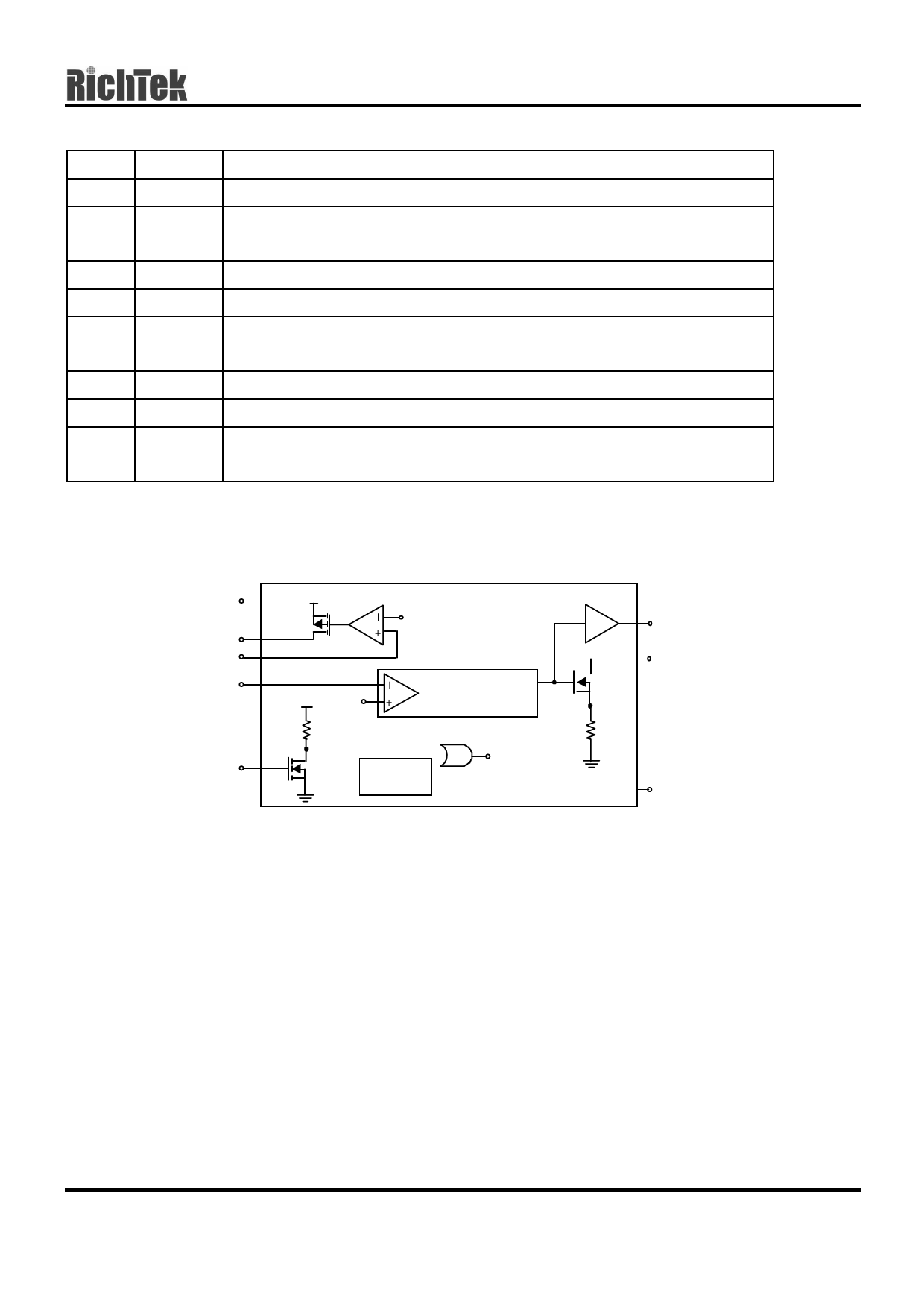
Function Block Diagram
VDD
LDOO
LFB
FB
CE
Q2 VDD
PMOS
RT9264
1.25V
VDD 1.25V
Loop Control Circuit
R2
Q3
Over Temp.
NMOS Detector
Shut Down
EXT
LX
Q1
NMOS
R1
GND
DS9264-00 December 2001
www.richtek-ic.com.tw
3
Share Link: 