BR24T1MFJ-3AM 查看數據表(PDF) - ROHM Semiconductor
零件编号
产品描述 (功能)
比赛名单
BR24T1MFJ-3AM Datasheet PDF : 32 Pages
| |||
BR24T1M-3AM
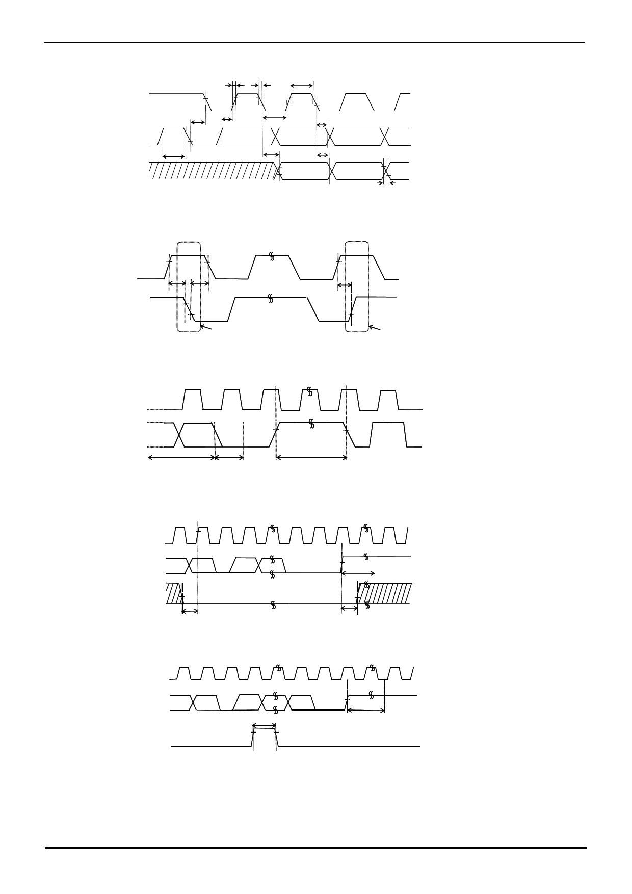
Serial Input / Output Timing
tR
tF1
tHIGH
SCL
tHD:STA
70%
70% 70%
30%
30%
tSU:DAT
tLOW
70%
30%
70%
70%
70%
30%
SDA
(INP(入U力 T))
tBUF
tPD
70%
30%
tHD:DAT
70%
30%
tDH
SDA
(OUTP(出 UT力) )
70%
30%
30%
(1) Input read at the rise edge of SCL
(2) Data output in sync with the fall of SCL
70%
30%
tF2
Figure 2-(a). Serial Input / Output Timing
70%
SCL
70%
70%
tSU:STA
tHD:STA
tSU:STO
SDA
70%
30%
30%
START CONDITION
Figure 2-(b). Start-Stop Bit Timing
STOP CONDITION
SCL
SDA
D0
write data
(n-th address)
ACK
70%
70%
tWR
STOP CONDITION START CONDITION
Figure 2-(c). Write Cycle Timing
SCL
70%
DATA(1)
SDA D1
D0 ACK
DATA(n)
WP
30%
ACK
70%
tWR
30%
tSU:WP
tHD:WP
STOP CONDITION
Figure 2-(d). WP Timing at Write Execution
SCL
SDA
WP
DATA(1)
D1
D0 ACK
DATA(n)
tHIGH:WP
70%
70%
ACK
70%
tWR
Figure 2-(e). WP Timing at Write Cancel
Datasheet
www..rohm.com
© 2016 ROHM Co., Ltd. All rights reserved.
TSZ22111・15・001
4/28
TSZ02201-0GFG0G100430-1-2
08.Jul.2016 Rev.001
Share Link: 