IRLML2803TR(2003) 查看數據表(PDF) - International Rectifier
零件编号
产品描述 (功能)
比赛名单
IRLML2803TR Datasheet PDF : 9 Pages
| |||
IRLML2803
Electrical Characteristics @ TJ = 25°C (unless otherwise specified)
Parameter
Min. Typ. Max. Units
Conditions
V(BR)DSS Drain-to-Source Breakdown Voltage
30 V VGS = 0V, ID = 250µA
∆V(BR)DSS/∆TJ Breakdown Voltage Temp. Coefficient 0.029 V/°C Reference to 25°C, ID = 1mA
RDS(on)
Static Drain-to-Source On-Resistance
0.25
0.40
Ω
VGS = 10V, ID = 0.91A
VGS = 4.5V, ID = 0.46A
VGS(th)
Gate Threshold Voltage
1.0 V VDS = VGS, ID = 250µA
gfs
Forward Transconductance
0.87 S VDS = 10V, ID = 0.46A
IDSS
Drain-to-Source Leakage Current
1.0
25
µA
VDS = 24V, VGS = 0V
VDS = 24V, VGS = 0V, TJ = 125°C
IGSS
Gate-to-Source Forward Leakage
Gate-to-Source Reverse Leakage
-100 nA VGS = -20V
100
VGS = 20V
Qg
Total Gate Charge
3.3 5.0
ID = 0.91A
Qgs
Gate-to-Source Charge
0.48 0.72 nC VDS = 24V
Qgd
Gate-to-Drain ("Miller") Charge
1.1 1.7
VGS = 10V, See Fig. 6 and 9
td(on)
Turn-On Delay Time
3.9
VDD = 15V
tr
td(off)
Rise Time
Turn-Off Delay Time
4.0
9.0
ns
ID = 0.91A
RG = 6.2Ω
tf
Fall Time
1.7
RD = 16Ω, See Fig. 10
Ciss
Input Capacitance
85
VGS = 0V
Coss
Output Capacitance
34 pF VDS = 25V
Crss
Reverse Transfer Capacitance
15
= 1.0MHz, See Fig. 5
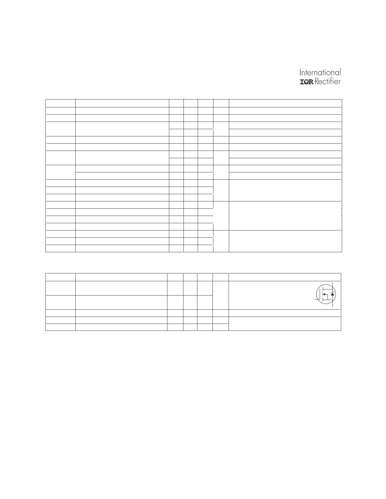
Source-Drain Ratings and Characteristics
Parameter
IS
Continuous Source Current
(Body Diode)
ISM
Pulsed Source Current
(Body Diode)
VSD
Diode Forward Voltage
trr
Reverse Recovery Time
Qrr
Reverse RecoveryCharge
Min. Typ. Max. Units
Conditions
0.54
7.3
MOSFET symbol
A showing the
integral reverse
p-n junction diode.
D
G
S
1.2 V TJ = 25°C, IS = 0.91A, VGS = 0V
26 40 ns TJ = 25°C, IF = 0.91A
22 32 nC di/dt = 100A/µs
Notes:
Repetitive rating; pulse width limited by
max. junction temperature. ( See fig. 11 )
Pulse width ≤ 300µs; duty cycle ≤ 2%.
ISD ≤ 0.91A, di/dt ≤ 120A/µs, VDD ≤ V(BR)DSS, Surface mounted on FR-4 board, t ≤ 5sec.
TJ ≤ 150°C
Share Link: 