74ABT543AN 查看數據表(PDF) - Philips Electronics
零件编号
产品描述 (功能)
比赛名单
74ABT543AN Datasheet PDF : 12 Pages
| |||
Philips Semiconductors
Octal latched transceiver with dual enable
(3-State)
Product specification
74ABT543A
AC CHARACTERISTICS
GND = 0V, tR = tF = 2.5ns, CL = 50pF, RL = 500Ω
SYMBOL
PARAMETER
WAVEFORM
tPLH
Propagation delay
tPHL
An to Bn, Bn to An
2
tPLH
Propagation delay
1
tPHL
LEBA to An, LEAB to Bn
2
tPZH
Output enable time
4
tPZL
OEBA to An, OEAB to Bn
5
tPHZ
Output disable time
4
tPLZ
OEBA to An, OEAB to Bn
5
tPZH
Output enable time
4
tPZL
EBA to An, EAB to Bn
5
tPHZ
Output disable time
4
tPLZ
EBA to An, EAB to Bn
5
AC SETUP REQUIREMENTS
GND = 0V, tR = tF = 2.5ns, CL = 50pF, RL = 500Ω
SYMBOL
PARAMETER
WAVEFORM
ts(H)
ts(L)
Setup time
An to LEAB, Bn to LEBA
3
th(H)
th(L)
Hold time
An to LEAB, Bn to LEBA
3
ts(H)
ts(L)
Setup time
An to EAB, Bn to EBA
3
th(H)
th(L)
Hold time
An to EAB, Bn to EBA
3
tw(L)
Latch enable pulse width, Low
3
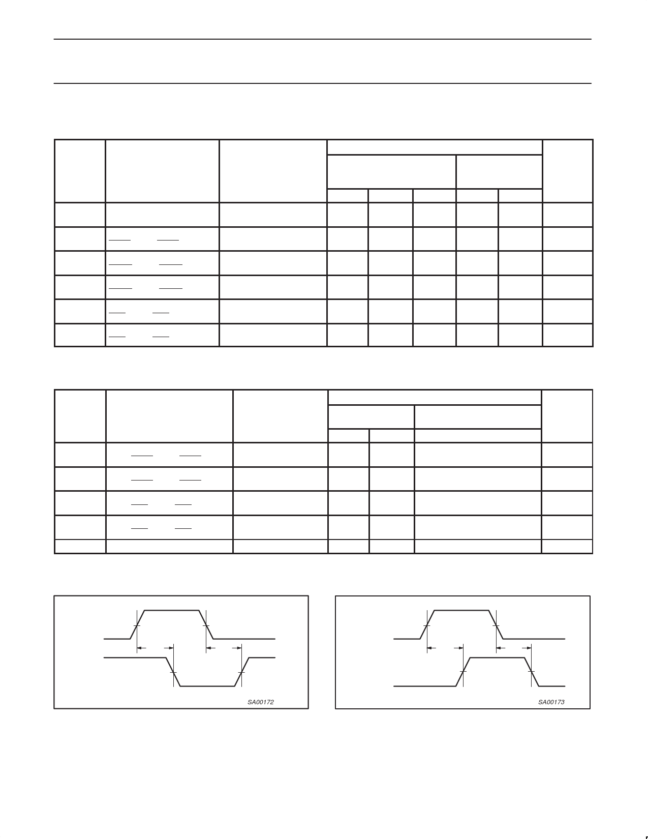
AC WAVEFORMS
VM = 1.5V, VIN = GND to 3.0V
VIN
VOUT
VM
tPHL
VM
VM
tPLH
VM
SA00172
Waveform 1. Propagation Delay For Inverting Output
LIMITS
Tamb = +25oC
VCC = +5.0V
Min
Typ
Max
1.0
2.9
4.5
1.9
3.6
5.2
1.0
3.4
5.1
2.1
4.3
6.0
1.0
3.2
5.1
2.0
4.3
5.9
2.0
4.0
5.7
1.0
3.0
4.6
1.0
3.4
5.1
2.0
4.4
6.1
2.0
3.6
5.4
1.0
3.0
4.6
Tamb = -40 to
+85oC
VCC = +5.0V ±0.5V
Min
Max
1.0
5.2
1.9
5.7
1.0
6.2
2.1
6.7
1.0
6.2
2.0
6.6
2.0
6.2
1.0
5.0
1.0
6.2
2.0
6.8
2.0
5.9
1.0
5.0
UNIT
ns
ns
ns
ns
ns
ns
Tamb = +25oC
VCC = +5.0V
Min
Typ
2.5
1.0
3.0
1.4
0.5
–0.8
0.5
–0.6
3.5
1.3
3.0
1.4
0.5
–0.8
0.5
–0.6
3.5
1.0
LIMITS
Tamb = -40 to +85oC
VCC = +5.0V ±0.5V
Min
2.5
3.0
0.5
0.5
3.5
3.0
0.5
0.5
3.5
UNIT
ns
ns
ns
ns
ns
VIN
VOUT
VM
tPLH
VM
VM
tPHL
VM
SA00173
Waveform 2. Propagation Delay For Non-Inverting Output
1998 Sep 24
6
Share Link: 