E749BPJ 查看數據表(PDF) - Semtech Corporation
零件编号
产品描述 (功能)
比赛名单
E749BPJ Datasheet PDF : 15 Pages
| |||
Edge749
TEST AND MEASUREMENT PRODUCTS
Application Information
Power Supplies
The Edge749 uses three power supplies: VDD, VCC and
VEE. VDD is the digital supply for all of the data inputs
and outputs. VCC and VEE are the analog power supplies
for the Edge749 drivers and comparators. In order to
protect the Edge749 and avoid damaging it, the following
power supply requirements must be satisifed at all times:
capacitor in parallel with a .001 µF chip capacitor. A
VCC and VEE plane, or at least a solid power bus, is
recommended for optimal performance.
VHIGH and VLOW Decoupling
Also,
VEE ≤ GND ≤ VDD ≤ VCC
VEE ≤ All Inputs ≤ VCC at all times
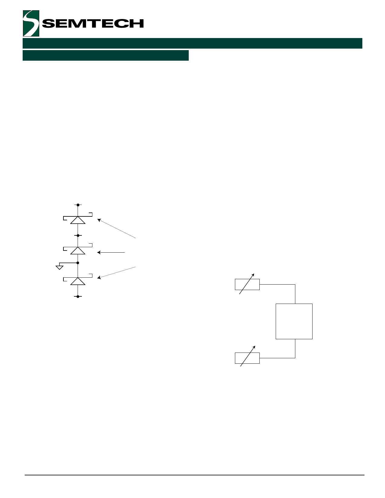
The three-Schottky diode configuration shown in Figure
5, used on a once-per-board basis, insures power supply
sequence and fault tolerance.
As the VHIGH and VLOW inputs are unbuffered and must
supply the driver output current, decoupling capacitors
for these inputs are recommended in proportion to the
amount of output current the application requires.
Expanding the Common Mode Range
VCC
Although the Edge749 can drive and receive 18 V swings,
these 18 V signals can be adjusted over an 21 V range.
By using programmable regulators V1 and V2 for the
VDD
VCC and VEE supplies (feasible because these two
analog power supplies do not supply driver output
1N5820 or
Equivalent
current), the Edge749 I/O range can be optimized for a
variety of applications (see Figure 6).
VEE
Figure 5. Power Supply Protection Scheme
Power-On Sequencing
1. VCC (substrate)
2. VEE
3. VDD
4. Inputs
Power-Off Sequencing
1. Inputs
2. VDD
3. VEE
4. VCC
V1
VCC
Edge 749
VDD
V2
Power Supplies Decoupling
Figure 6.
VDD, which provides the digital power, should be
decoupled to GND with a .1 µF chip capacitor in parallel
with a .001 µF chip capacitor. The bypass capacitors
should be as close to the device as possible. Power and
ground planes are recommended to provide a low
inductance return path.
There are three rules which govern the supplies V1 and
V2:
1) +10V < V1 < +18V
2) –3V < V2 < 0V
3) (V1 – V2) < +18V.
VCC and VEE, which power the DUT drivers and receivers,
should also be decoupled to GND with a .1 µF chip
Revision 3 / October 21, 2002
6
www .semtech.com
Share Link: 