MC74F543N 查看數據表(PDF) - Motorola => Freescale
零件编号
产品描述 (功能)
比赛名单
MC74F543N Datasheet PDF : 4 Pages
| |||
MC74F543
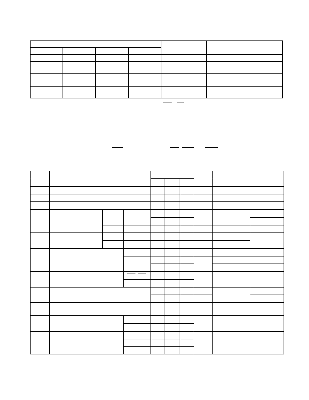
FUNCTION TABLE
Inputs
OEXX
EXX
LEXX
Data
Outputs
Status
H
X
X
X
Z
Outputs disabled
L
H
L
l
L
H
L
h
Z
Outputs disabled
Z
Data latched
L
L
H
l
L
L
H
h
L
H
Data latched
L
L
L
L
L
L
L
H
L
H
Transparent
H = HIGH voltage level: h = HIGH state must be present one set-up time before the LOW-to-HIGH transition of LEXX or EXX (XX = AB or BA): L = LOW Voltage Level:
I = LOW state must be present one set-up time before the LOW-to-HIGH transition of LEXX or EXX (XX = AB or BA): X = Don’t care: Z = HIGH impedance state.
FUNCTIONAL DESCRIPTION
The MC74F543 contains two sets of eight D-type latches,
with separate input and controls for each set. For data flow
from A to B, for example, the A-to-B Enable (EAB) Input must
be LOW in order to enter data from A0 – A7 or take data from
B0 – B7, as indicated in the Function Table. With EAB LOW, a
LOW signal on the A-to-B Latch Enable (LEAB) input makes
the A-to-B latches transparent; a subsequent LOW-to-HIGH
transition of the LEAB signal puts the A latches in the storage
mode and their outputs no longer change with the A inputs.
With EAB and OEAB both LOW, the 3-State B output buffers
are active and reflects the data present at the output of the A
latches. Control of data flow from B to A is similar, but using
the EBA, LEBA, and OEBA inputs.
DC CHARACTERISTICS OVER OPERATING TEMPERATURE RANGE (unless otherwise specified)
Limits
Symbol
Parameter
Min Typ Max Unit
Test Conditions
VIH
VIL
VIK
VOH
VOL
IIH
IIL
Input HIGH Voltage
2.0
V
Input LOW Voltage
0.8
V
Input Clamp Diode Voltage
–0.73 – 1.2
V
2.4
A0 – A7
74
V
Output HIGH Voltage
2.7 3.4
B0 – B7
74
2.0
V
Output LOW Voltage
A0 – A7
74
B0 – B7
74
0.35 0.5
V
0.4 0.55
V
I/O Pins
1.0 mA
Input HIGH Current
Control Pins
100
µA
20
Input LOW Current
EAB, EBA
Other Inputs
– 1.2
mA
– 0.6
Guaranteed Input HIGH Voltage
Guaranteed Input LOW Voltage
VCC = MIN, IIN = – 18 mA
IOH = – 3.0 mA
VCC = 4.5 V
VCC = 4.75 V
IOH = – 15 mA
VCC = 4.5 V
IOL = 24 mA
IOL = 64 mA
VCC = MIN
VCC = MAX, VIN = 5.5 V
VCC = MAX, VIN = 7.0 V
VCC = MAX, VIN = 2.7 V
VCC = MAX, VIN = 0.5 V
IOZH
IOZL
Off-State Output Current,
High-Level Voltage Applied
Off-State Output Current,
Low-Level Voltage Applied
70
µA
1.0 mA
– 600 µA
VCC = MAX
VOUT = 2.7 V
VOUT = 5.5 V
VCC = MAX, VOUT = 0.5 V
An Outputs – 60
IOS
Output Short Circuit Current (Note 2)
Bn Outputs – 100
–150
mA
–225
VCC = MAX, VOUT = 0 V
ICCH
70 100
ICC
Total Supply Current
ICCL
95 125 mA VCC = MAX
ICCZ
95 125
NOTES:
1. For conditions shown as MIN or MAX, use the appropriate value specified under recommended operating conditions for the applicable device type.
2. Not more than one output should be shorted at a time, nor for more than 1 second.
FAST AND LS TTL DATA
4-213
Share Link: 