HD74ACT164 查看數據表(PDF) - Hitachi -> Renesas Electronics
零件编号
产品描述 (功能)
比赛名单
HD74ACT164 Datasheet PDF : 10 Pages
| |||
HD74AC164/HD74ACT164
Mode Select Table
Inputs
Outputs
Operating Mode
MR
A
B
Q0
Q1 to Q7
Reset (Clear)
L
X
X
L
L to L
Shift
H:
L:
X:
qn :
H
L
L
L
q0 to q6
H
L
H
L
q0 to q6
H
H
L
L
q0 to q6
H
H
H
H
q0 to q6
High Voltage Level
Low Voltage Level
Immaterial
Lower case letters indicate the state of the referenced input or output one setup time prior to the
Low-to-High clock transition.
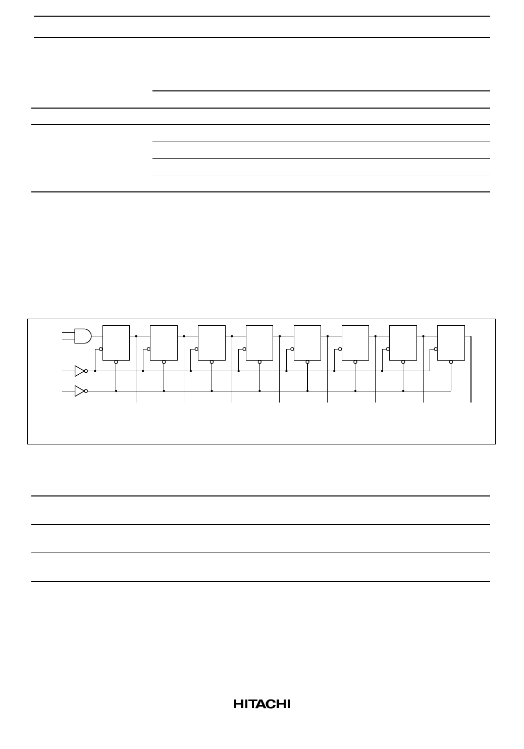
Logic Diagram
A
B
DQ
DQ
DQ
DQ
DQ
DQ
DQ
DQ
CD
CD
CD
CD
CD
CD
CD
CD
CP
MR
Q0
Q1
Q2
Q3
Q4
Q5
Q6
Q7
Please note that this diagram is provided only for the understanding of logic operations and should not be
used to estimate propagation delays.
DC Characteristics (unless otherwise specified)
Item
Symbol Max
Unit
Maximum quiescent supply current ICC
80
µA
Maximum quiescent supply current ICC
8.0
µA
Maximum additional ICC/input
(HD74ACT164)
I CCT
1.5
mA
Condition
VIN = VCC or ground, VCC = 5.5 V,
Ta = Worst case
VIN = VCC or ground, VCC = 5.5 V,
Ta = 25°C
VIN = VCC – 2.1 V, VCC = 5.5 V,
Ta = Worst case
3
Share Link: 