AD9430/PCB-CMOS 查看數據表(PDF) - Analog Devices
零件编号
产品描述 (功能)
比赛名单
AD9430/PCB-CMOS Datasheet PDF : 20 Pages
| |||
PRELIMINARY TECHNICAL DATA
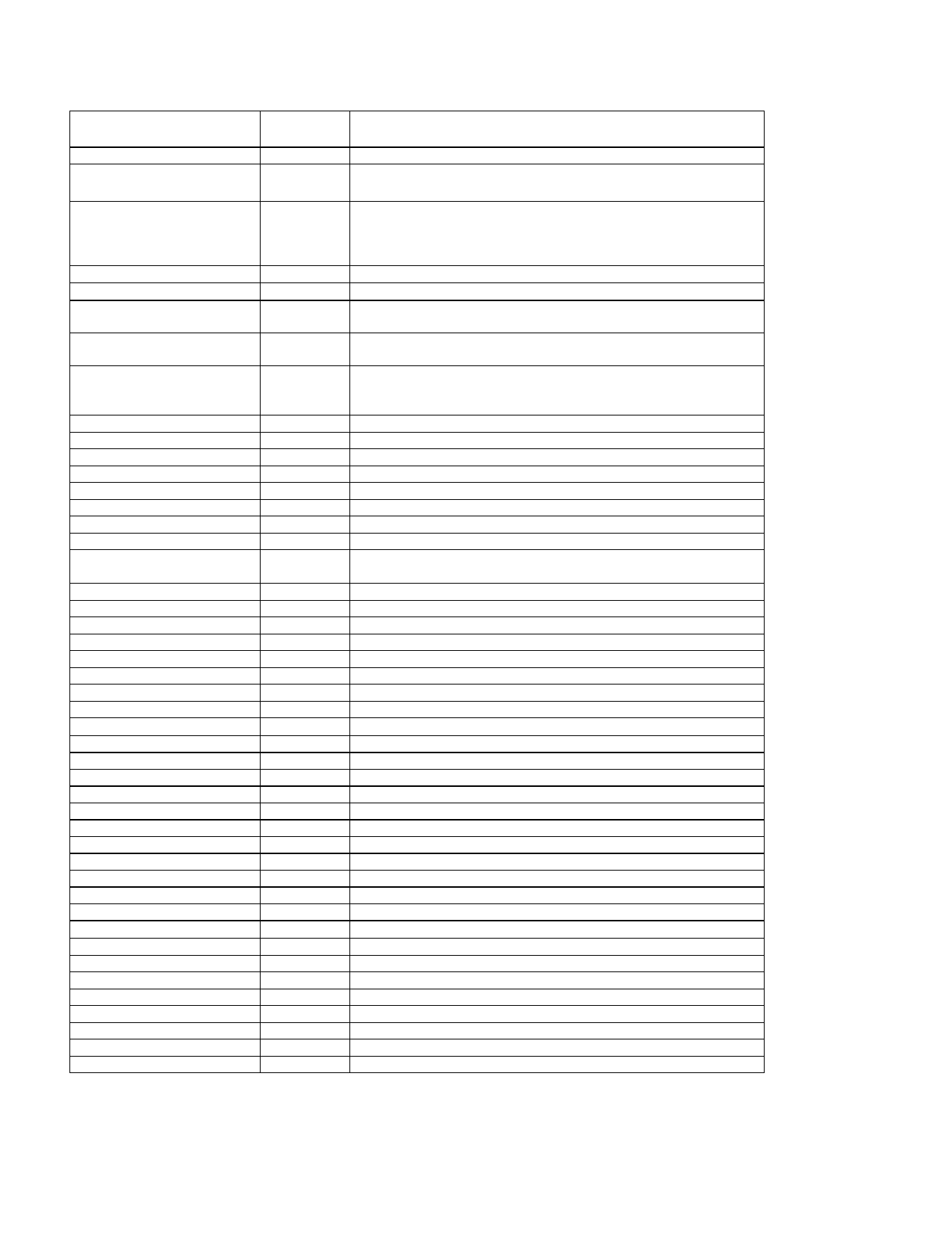
PIN FUNCTION DESCRIPTIONS (LVDS mode )
LVDS Mode
Pin Number
Name
Function in LVDS Mode
2,42,43,44,45,46
DNC
Do not connect
1
S5
Full Scale Adjust pin : ‘1’ sets FS =.766 Vpp differential,
‘0’ sets FS = 1.533 Vpp differential
3
S4
Interlaced or parallel output mode. (only in Dual Port mode
operation) HIGH = data arrives in channel A at falling edge of clock
and data arrives in channelA at rising edge of clock. LOW = data
arrives in channels A and B at rising edge of clock.
5
S2
Output Mode select. Low = Dual Port, CMOS; High = LVDS
6
S1
Data format select. Low = Binary, High = Two’s compliment
7
LVDSBIAS Sets LVDS Output Current = 3.5mA
(Place 3.7K RSET resistor from LVDSBIAS to ground)
8,14,15,18,19,24,27,28,29,34, AVDD
39,40,88,89,90,94,95,98,99
3.3V analog supply. (3.0V to 3.6V)
4,9,12,13,16,17,20,23,25,26,3 AGND
Analog Ground
0,31,35,38,41,86,87,91,92,93,
96,97,100
10
SENSE
Control Pin for Reference , Full Scale
11
VREF
1.235 Reference I/O - function dependent on REFSENSE
21
VIN+
Analog input – true.
22
VIN-
Analog input – compliment.
32
DS+
Data sync (input) – Not used in LVDS mode.Tie LOW .
33
DS-
Data sync (input) – compliment. Not used in LVDS mode.Tie HIGH.
36
ENC+
Clock input – true.
(LVPECL levels)
37
ENC-
Clock input – compliment. (LVPECL levels)
47,54,62,75,83
DrVDD
3.3V digital output supply.
48,53,61,67,74,82
49
50
51
52
55
56
57
58
59
60
63
64
65
66
68
69
70
71
72
73
76
77
78
79
80
81
84
85
DrGND
D0_C
D0_T
D1_C
D1_T
D2_C
D2_T
D3_C
D3_T
D4_C
D4_T
DCO-
DCO+
D5_C
D5_T
D6_C
D6_T
D7_C
D7_T
D8_C
D8_T
D9_C
D9_T
D10_C
D10_T
D11_C
D11_T
OR_C
OR_T
Digital ground.
D0 complement output bit (LSB) (LVDS Levels)
D0 true output bit (LSB)
(LVDS Levels)
D1 complement output bit
(LVDS Levels)
D1 true output bit
(LVDS Levels)
D2 complement output bit (LVDS Levels)
D2 true output bit (LVDS Levels)
D3 complement output bit (LVDS Levels)
D3 true output bit (LVDS Levels)
D4 complement output bit (LVDS Levels)
D4 true output bit (LVDS Levels)
Data Clock output – compliment. (LVDS Levels)
Data Clock output – true.
(LVDS Levels)
D5 complement output bit (LVDS Levels)
D5 true output bit (LVDS Levels)
D6 complement output bit (LVDS Levels)
D6 true output bit (LVDS Levels)
D7 complement output bit (LVDS Levels)
D7 true output bit (LVDS Levels)
D8 complement output bit (LVDS Levels)
D8 true output bit (LVDS Levels)
D9 complement output bit (LVDS Levels)
D9 true output bit (LVDS Levels)
D10 complement output bit (LVDS Levels)
D10 true output bit (LVDS Levels)
D11 complement output bit (LVDS Levels) MSB
D11 true output bit (LVDS Levels) MSB
Overrange complement output bit (LVDS Levels)
Overrange true output bit (LVDS Levels)
AD9430
REV. PrG 4/01/2002
-9-
Share Link: 