MC74LVX32DT 查看數據表(PDF) - ON Semiconductor
零件编号
产品描述 (功能)
比赛名单
MC74LVX32DT Datasheet PDF : 8 Pages
| |||
MC74LVX32
ÎÎÎÎÎÎÎÎÎÎÎÎÎÎÎÎÎÎÎÎÎÎÎÎÎÎÎÎÎÎÎÎÎ AC ELECTRICAL CHARACTERISTICS (Input tr = tf = 3.0ns)
ÎÎÎÎÎÎÎÎÎÎÎÎÎÎÎÎÎÎÎÎÎÎÎÎÎÎÎÎÎÎÎÎÎ TA = 25°C
TA = – 40 to 85°C
ÎÎÎÎÎÎÎÎÎÎÎÎÎÎÎÎÎÎÎÎÎÎÎÎÎÎÎÎÎÎÎÎÎ Symbol
Parameter
Test Conditions
Min
Typ
Max
Min
Max Unit
ÎÎÎÎÎÎÎÎÎÎÎÎÎÎÎÎÎÎÎÎÎÎÎÎÎÎÎÎÎÎÎÎÎ tPLH,
tPHL
Propagation Delay, Input to
Output
VCC = 2.7V
CL = 15pF
CL = 50pF
5.8
10.7
1.0
13.5 ns
8.3
14.2
1.0
17.0
ÎÎÎÎÎÎÎÎÎÎÎÎÎÎÎÎÎÎÎÎÎÎÎÎÎÎÎÎÎÎÎÎÎ VCC=3.3±0.3V CL=15pF
ÎÎÎÎÎÎÎÎÎÎÎÎÎÎÎÎÎÎÎÎÎÎÎÎÎÎÎÎÎÎÎÎÎ CL = 50pF
4.4
6.6
1.0
8.0
6.9
10.1
1.0
11.5
ÎÎÎÎÎÎÎÎÎÎÎÎÎÎÎÎÎÎÎÎÎÎÎÎÎÎÎÎÎÎÎÎÎ tOSHL
ÎÎÎÎÎÎÎÎÎÎÎÎÎÎÎÎÎÎÎÎÎÎÎÎÎÎÎÎÎÎÎÎÎ tOSLH
Output–to–Output Skew
(Note NO TAG)
VCC = 2.7V
VCC = 3.3 ±0.3V
CL = 50pF
CL = 50pF
1.5
1.5
ns
1.5
1.5
ÎÎÎÎÎÎÎÎÎÎÎÎÎÎÎÎÎÎÎÎÎÎÎÎÎÎÎÎÎÎÎÎÎ 1. Skew is defined as the absolute value of the difference between the actual propagation delay for any two separate outputs of the same device.
The specification applies to any outputs switching in the same direction, either HIGH–to–LOW (tOSHL) or LOW–to–HIGH (tOSLH); parameter
guaranteed by design.
CAPACITIVE CHARACTERISTICS
ÎÎÎÎÎÎÎÎÎÎÎÎÎÎÎÎÎÎÎÎÎÎÎÎÎÎÎÎÎÎÎÎÎÎÎÎÎÎÎÎÎÎÎÎÎÎÎÎÎÎÎÎÎÎÎÎÎÎÎÎÎÎÎÎÎÎ Symbol
ÎÎÎÎÎÎÎÎÎÎÎÎÎÎÎÎÎÎÎÎÎÎÎÎÎÎÎÎÎÎÎÎÎ Cin
ÎÎÎÎÎÎÎÎÎÎÎÎÎÎÎÎÎÎÎÎÎÎÎÎÎÎÎÎÎÎÎÎÎÎÎÎÎÎÎÎÎÎÎÎÎÎÎÎÎÎÎÎÎÎÎÎÎÎÎÎÎÎÎÎÎÎ CPD
Parameter
Input Capacitance
Power Dissipation Capacitance (Note NO TAG)
TA = 25°C
Min
Typ
Max
4
10
14
TA = – 40 to 85°C
Min
Max Unit
10
pF
pF
2. CPD is defined as the value of the internal equivalent capacitance which is calculated from the operating current consumption without load.
Average operating current can be obtained by the equation: ICC(OPR) = CPD VCC fin + ICC/4 (per gate). CPD is used to determine the no–load
dynamic power consumption; PD = CPD VCC2 fin + ICC VCC.
NOISE CHARACTERISTICS (Input tr = tf = 3.0ns, CL = 50pF, VCC = 3.3V, Measured in SOIC Package)
TA = 25°C
Symbol
Characteristic
Typ
Max
Unit
VOLP Quiet Output Maximum Dynamic VOL
0.3
0.5
V
VOLV Quiet Output Minimum Dynamic VOL
–0.3
–0.5
V
VIHD Minimum High Level Dynamic Input Voltage
2.0
V
VILD Maximum Low Level Dynamic Input Voltage
0.8
V
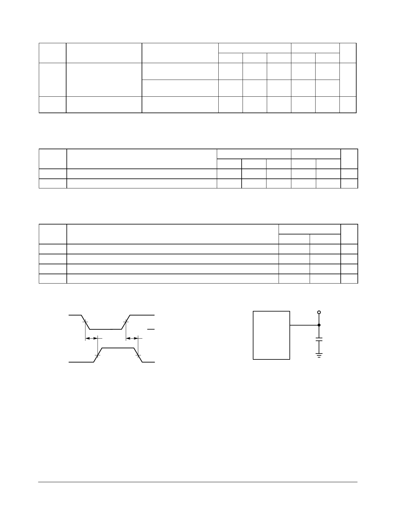
A or B
50%
O
tPLH
50% VCC
VCC
GND
tPHL
Figure 3. Switching Waveforms
DEVICE
UNDER
TEST
TEST POINT
OUTPUT
CL*
*Includes all probe and jig capacitance
Figure 4. Test Circuit
http://onsemi.com
4
Share Link: 