PI5C3257L 查看數據表(PDF) - Pericom Semiconductor
零件编号
产品描述 (功能)
比赛名单
PI5C3257L Datasheet PDF : 6 Pages
| |||
PI5C3257
Quad 2:1 Mux/DeMux BusSwitch
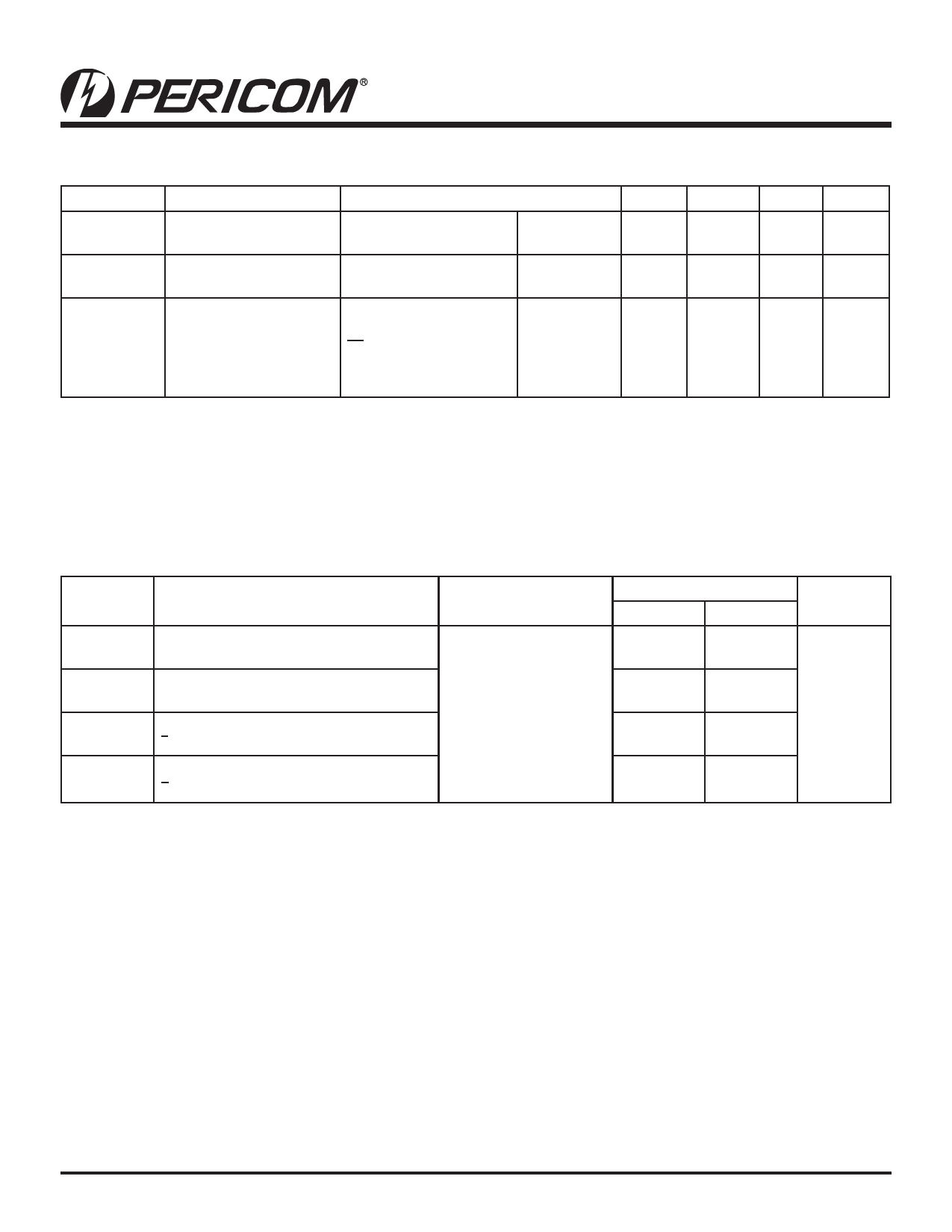
Power Supply Characteristics
Parameters
Description
Test Conditions(1)
Min. Typ(2) Max. Units
ICC
∆ICC
Quiescent Power
Supply Current
Supply Current per
Input @ TTL HIGH
VCC = Max.
VCC = Max.
VIN = GND
or VCC
VIN = 3.4V(3)
0.1
3.0
µA
2.5
mA
ICCD
Supply Current per
Input per MHz(4)
VCC = Max.,
I and Y Pins Open
BE = GND
Control Input Toggling
50% Duty Cycle
0.25
mA/
MHz
Notes:
1. For Max. or Min. conditions, use appropriate value specified under Electrical Characteristics for the applicable device.
2. Typical values are at VCC = 5.0V, +25°C ambient.
3. Per TTL driven input (VIN = 3.4V, control inputs only); I and Y pins do not contribute to ICC.
4. This current applies to the control inputs only and represent the current required to switch internal capacitance at the specified frequency. The I
and Y inputs generate no significant AC or DC currents as they transition. This parameter is not tested, but is guaranteed by design.
Switching Characteristics over Operating Range
Parameters
Description
tIY
Propagation Delay(1,2)
In to Yn
tSY
Bus Select Time
Sn to Yn
tPZH
Bus Enable Time
tPZL
E to Yn
tPHZ
Bus Disable Time
tPLZ
E to Yn
Conditions
CL = 50pF
RL = 500Ω
Com.
Min.
Max.
0.25
0.5
5.2
0.5
4.8
0.5
5.0
Units
ns
Notes:
1. This parameter is guaranteed but not tested on Propagation Delays.
2. The bus switch contributes no propagational delay other than the RC delay of the On-Resistance of the switch and the load capacitance. The
time constant for the switch alone is of the order of 0.25ns for 50pF load. Since this time constant is much smaller than the rise/fall times of
typical driving signals, it adds very little propagational delay to the system. Propagational delay of the bus switch when used in a system is
determined by the driving circuit on the driving side of the switch and its interaction with the load on the driven side.
06-0240
3
PS7018G
11/04/06
Share Link: 