HCC4043 查看數據表(PDF) - STMicroelectronics
零件编号
产品描述 (功能)
比赛名单
HCC4043 Datasheet PDF : 13 Pages
| |||
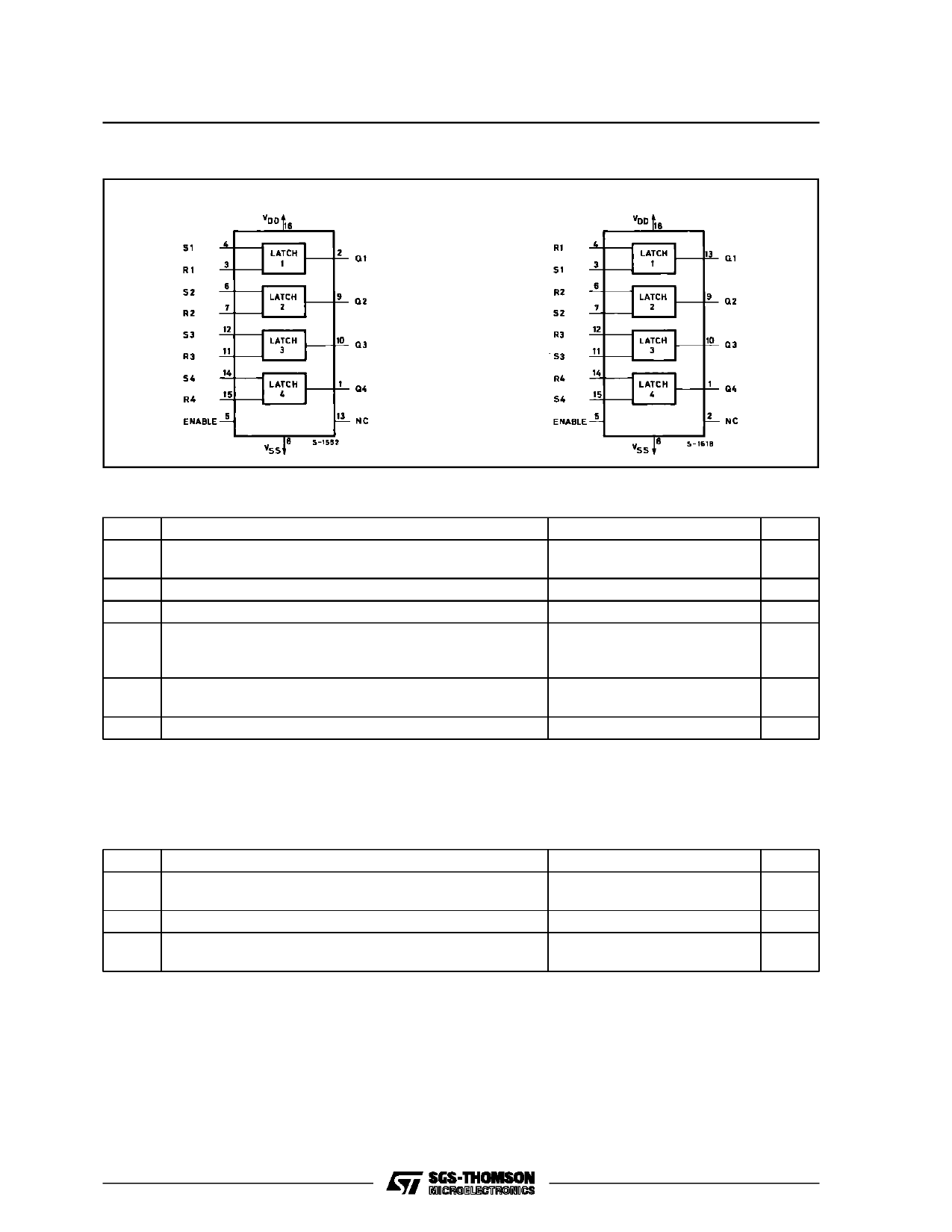
HCC/HCF4043B/4044B
FUNCTIONAL DIAGRAMS
4043B
4044B
ABSOLUTE MAXIMUM RATINGS
Symbol
Parameter
Value
Unit
V DD* Supply Voltage : HC C Types
H C F Types
– 0.5 to + 20
V
– 0.5 to + 18
V
Vi Input Voltage
II
DC Input Current (any one input)
– 0.5 to VDD + 0.5
V
± 10
mA
Pt o t Total Power Dissipation (per package)
Dissipation per Output Transistor
for To p = Full Package-temperature Range
T o p Operating Temperature : HCC Types
H CF Types
200
mW
100
mW
– 55 to + 125
°C
– 40 to + 85
°C
Ts tg Storage Temperature
– 65 to + 150
°C
Stresses above those listed under ”Absolute Maximum Ratings” may cause permanent damage to the device. This is a stress
rating only and functional operation of the device at these or any other conditions above those indicated in the operational sections
of this specification is not implied. Exposure to absolute maximum rating conditions for external periods may affect device reliabili ty.
* All voltage values are referred to VSS pin voltage.
RECOMMENDED OPERATING CONDITIONS
Symbol
Parameter
VDD Supply Voltage : HC C Types
H C F Types
VI Input Voltage
T o p Operating Temperature : H CC Types
H C F Types
Value
3 to 18
3 to 15
0 to VDD
– 55 to + 125
– 40 to + 85
Unit
V
V
V
°C
°C
2/13
Share Link: 