CMX838 查看數據表(PDF) - MX-COM Inc
零件编号
产品描述 (功能)
比赛名单
CMX838 Datasheet PDF : 70 Pages
| |||
FRS/PMR446/GMRS Family Radio Processor
8
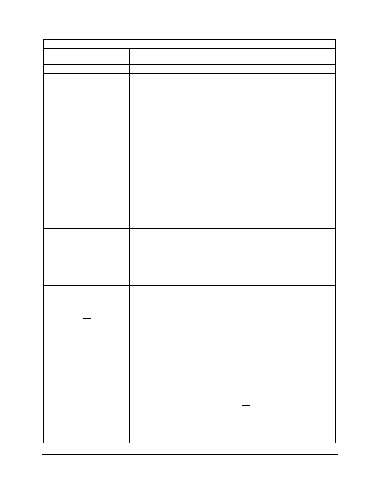
2 Signal List
CMX838 Advance Information
Package
Pin No.
E1/D1
1
2
Signal
Name
Type
RXIN
AUX I/O
input
input/output
3
MICOUT
4
MICIN
5
CPOUT
6
ISET
7
SVDD
8
-RFIN
9
+RFIN
10
SVSS
11
REFIN
12
XTAL
13
XTAL
14
CS
15
IRQ
output
input
output
input
power
input
input
power
input
input
output
input
output
16
RPLY DATA
17
CMD DATA
output
input
Description
Receive input for both audio and subaudio signals.
When configured as an input this pin can be used to route
externally generated ringing or alert signals to the Rx and
Tx audio paths.
When configured as an output this pin allows for
monitoring internally generated ringing or alert signals.
See Section 4.2.4.5.3
Microphone amplifier feedback output.
Microphone amplifier input. This is the inverting input to a
high gain opamp, suitable for use with common
microphones.
Synthesizer charge pump output. Apply to external loop
filter that drives the control input of an external VCO
Synthesizer charge pump current control. Connect via
external resistor to SVSS to set charge pump current.
Synthesizer positive supply. This signal must be
decoupled to SVSS by a capacitor mounted close to the
device pins.
Synthesizer RF negative input. Connect this pin to SVSS
(synthesizer common) when a non-differential input signal
is applied to +RFIN.
Synthesizer RF positive input.
Synthesizer negative supply.
Synthesizer reference oscillator input.
The input to the on-chip oscillator, for external Xtal circuit
or clock. This input should be connected to VSS, Circuit
Common, when the device is configured to generate the
XTAL clock internally from the REFIN clock.
Inverted output of the on-chip crystal oscillator. This pin
should not be connected (left open) when the device is
configured to generate the XTAL clock internally from the
REFIN clock.
C-BUS select data loading control function input. This
input controls C-BUS transfer initiation, completion and
cancellation.
Interrupt output, logic '0' active level. This is a 'wire-
Orable' output, enabling the connection of multiple
peripherals to 1 interrupt port on an external µController.
This pin has a low impedance pull-down to logic "0" when
active and a high-impedance when inactive. An external
pull-up resistor is required. Interrupt outputs may be
configured via mask bits via C-BUS commands.
Reply data output to C-BUS serial control port. Output
reply data bytes are synchronized to the CLK clock input
under the control of the CS input. This 3-state output is
held at high impedance when not driving output data.
Command data input to C-BUS serial control port. Data is
loaded into this device in 8-bit bytes, MSB (D7) first, and
LSB (D0) last, synchronized to the CLK clock input.
¤2001 MX-COM, Inc.
www.mxcom.com Tel: 800 638 5577 336 744 5050 Fax: 336 744 5054
Doc. # 20480221.002
4800 Bethania Station Road, Winston-Salem, NC 27105-1201 USA All trademarks and service marks are held by their respective companies.
Share Link: 