GS71116J 查看數據表(PDF) - Giga Semiconductor
零件编号
产品描述 (功能)
比赛名单
GS71116J Datasheet PDF : 15 Pages
| |||
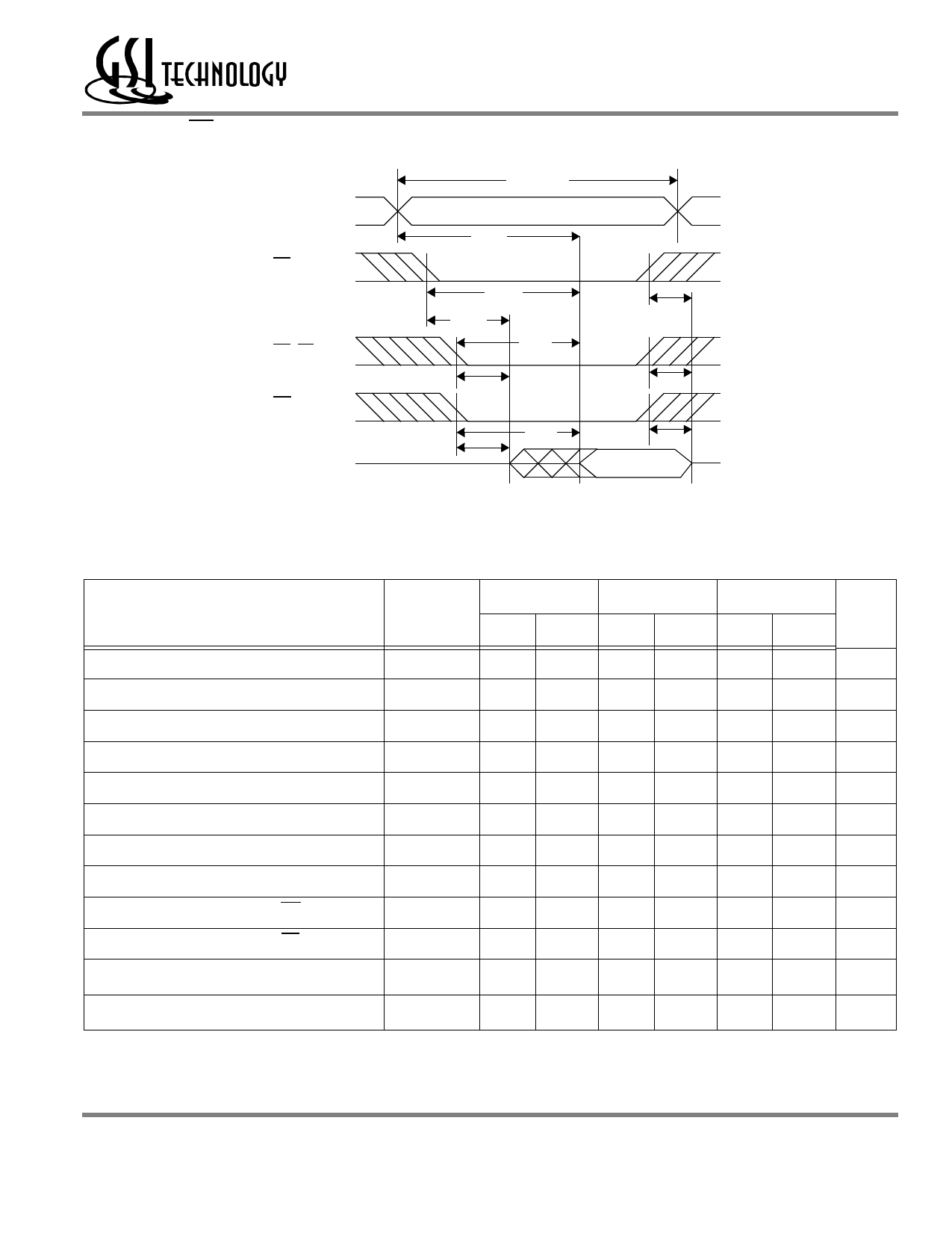
Read Cycle 2: WE = VIH
Address
CE
UB, LB
OE
Data Out
tRC
tAA
tAC
tLZ
tAB
tBLZ
tOE
tOLZ
High impedance
tHZ
tBHZ
tOHZ
Data valid
GS71116TP/J/U
Write Cycle
Parameter
Symbol
Write cycle time
tWC
Address valid to end of write
tAW
Chip enable to end of write
tCW
Byte enable to end of write
tBW
Data set up time
tDW
Data hold time
tDH
Write pulse width
tWP
Address set up time
tAS
Write recovery time (WE)
tWR
Write recovery time (CE)
tWR1
Output Low Z from end of write
tWLZ*
Write to output in High Z
tWHZ*
* These parameters are sampled and are not 100% tested
-10
-12
-15
Unit
Min Max Min Max Min Max
10
---
12
---
15
---
ns
7
---
8
---
10
---
ns
7
---
8
---
10
---
ns
7
---
8
---
10
---
ns
5
---
6
---
7
---
ns
0
---
0
---
0
---
ns
7
---
8
---
10
---
ns
0
---
0
---
0
---
ns
0
---
0
---
0
---
ns
0
---
0
---
0
---
ns
3
---
3
---
3
---
ns
---
4
---
5
---
6
ns
Rev: 1.06 6/2000
8/15
Specifications cited are subject to change without notice. For latest documentation see http://www.gsitechnology.com.
© 1999, Giga Semiconductor, Inc.
Share Link: 