SP6642EU 查看數據表(PDF) - Signal Processing Technologies
零件编号
产品描述 (功能)
比赛名单
SP6642EU Datasheet PDF : 16 Pages
| |||
PERFORMANCE CHARACTERISTICS (continued)
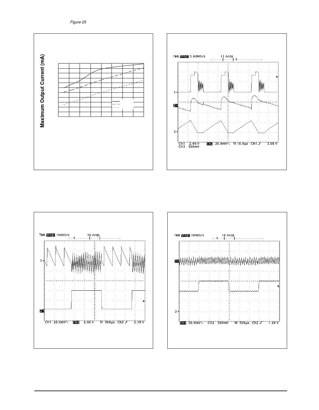
Refer
to
the
circuit
in
Figure
25
with
V
BATT
=
1.2V,
R1
+
R2
=
1MΩ,
and
T
AMB
=
+25OC
unless
otherwise
noted.
22
20
18
16
14
12
10
8
6
Vout = 2.4V
Vout = 3.3V
4
Vout = 5V
2
0
0.8 0.9 1.0 1.1 1.2 1.3 1.4 1.5 1.6
Input Voltage (V)
10msec/div
Figure 13. Maximum Output Current vs. Input Voltage
where L1=150µH, TDK NLC565050T-151K
Figure 14. Switching Waveforms:
VOUT=3.3V, VIN=1.2V, IOUT=12mA where
1: LX, 2V/div, L1=TDK NKLC565050T-151K
2: VOUT, 20mV/div, 3.3V DC offset
3: Inductor Current, 100mA/div
500µsec/div
500µsec/div
Figure 15. Load-Transient Response:
VOUT=3.3V, VBATT=1.2V where
1: VOUT, 20mV/div, 3.3V DC offset
2: LOAD, 2mA to 20mA, 10mA/div
Figure 16. Line-Transient Response:
VOUT=3.3V, LOAD=15mA where
1: VOUT, 50mV/div, 3.3V DC offset
2: VBATT, 1V to 5V, 500mV/div
Rev. 10-6-00
SP6642/6643 High Efficiency Step-Up DC-DC Converter
7
© Copyright 2000 Sipex Corporation
Share Link: 