MSM6996H 查看數據表(PDF) - Oki Electric Industry
零件编号
产品描述 (功能)
比赛名单
MSM6996H Datasheet PDF : 21 Pages
| |||
¡ Semiconductor
MSM6996H/6996V/6997H/6997V/6998/6999
PIN AND FUNCTIONAL DESCRIPTIONS
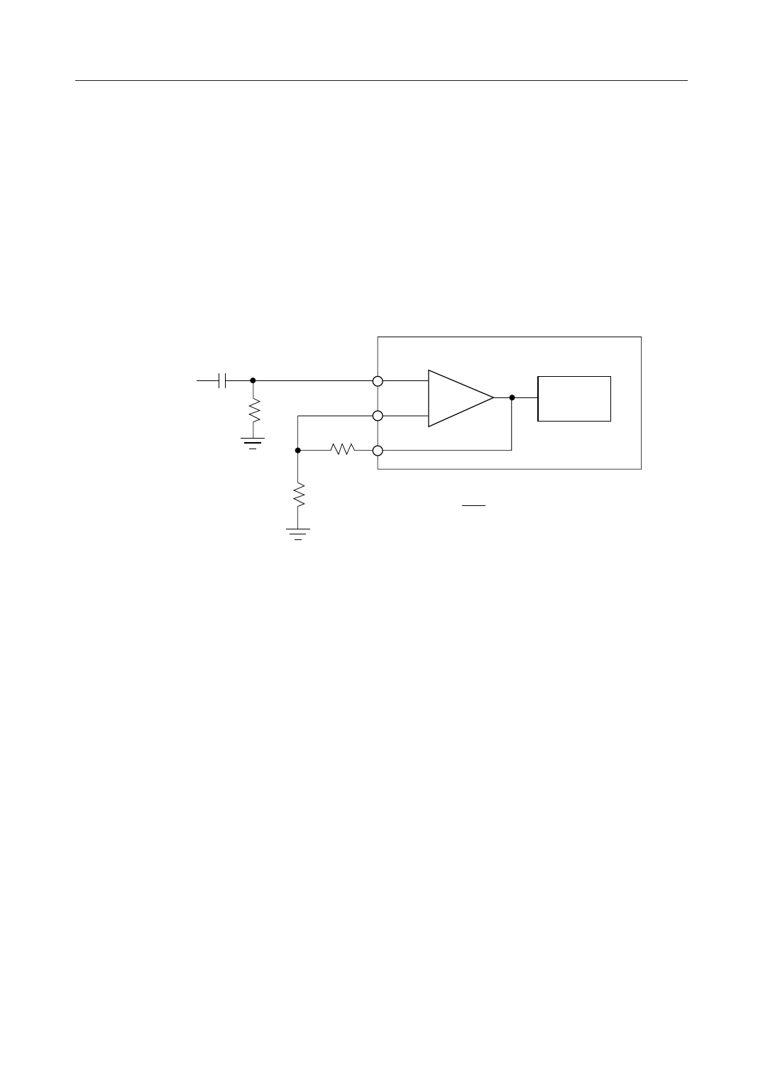
AIN+, AIN–, GSX
These three pins are used for the transmit level adjustment.
AIN+ is a non-inverting analog input pin which is connected to the non-inverting input of a transmit
amplifier.
AIN– is an inverting analog input pin which is connected to the inverting input of the transmit
amplifier.
GSX is a transmit amplifier output pin.
Adjustment can be done by following method.
Analog C1
Input
R1
AIN+
+
AIN–
–
R2
GSX
RC
Active
Filter
R3
R2
Gain = 1 + R3 < 10
AG
Notes: 1. R2 + R3 > 10 kW
2. When the DC off-set voltage of analog input is more than 20 mV, C1 and R1 should
provide for DC blocking.
In this case, cut-off frequency of HPF, composed by R1 and C1, should be less than 30 Hz.
3. R1 should be less than 20 kW
AG
AG is an analog ground.
AG is connected to the analog system ground.
AOUT
AOUT is the analog signal output pin for the MSM6996H/V and MSM6997H/V.
The output voltage range is 5 VPP. This output can drive the 600 W resistor.
AOUT+, AOUT–
Analog output for the MSM6998 and MSM6999.
The output signal amplitudes are 5 VPP. The AOUT– output is inverted to the AOUT+ output. These
outputs can drive a 600 W impedance.
VDD
VDD is the positive power supply.
The voltage supplied to this pin should be +5 V ±5%.
5/21
Share Link: 