W166(2001) 查看數據表(PDF) - Cypress Semiconductor
零件编号
产品描述 (功能)
比赛名单
W166 Datasheet PDF : 8 Pages
| |||

W166
Pin Definitions
Pin Name Pin No.
CLKOUT
7
CLKIN
1
NC
2
SSON#
8
FS0:1
6, 4
VDD
5
GND
3
Pin
Type
O
I
NC
I
I
P
G
Pin Description
Output Modulated Frequency: Frequency modulated copy of the reference input
(SSON# asserted).
External Reference Frequency Input: Clock input.
No Connect: This pin must be left unconnected.
Spread Spectrum Control (Active LOW): Asserting this signal (active LOW) turns the
internal modulation waveform on. This pin has an internal pull-down resistor.
Frequency Selection Bits 0,1: These pins select the frequency spreading characteris-
tics. Refer to Table 1. These pins have internal pull-up resistors.
Power Connection: Connected to 3.3V or 5V power supply.
Ground Connection: This should be connected to the common ground plane.
Functional Description
The W166 uses a Phase-Locked Loop (PLL) to frequency
modulate an input clock. The result is an output clock whose
frequency is slowly swept over a narrow band near the input
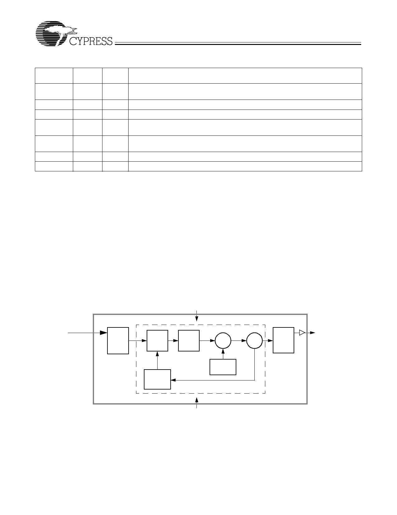
signal. The basic circuit topology is shown in Figure 1. The
input reference signal is divided by Q and fed to the phase
detector. A signal from the VCO is divided by P and fed back
to the phase detector also. The PLL will force the frequency of
the VCO output signal to change until the divided output signal
and the divided reference signal match at the phase detector
input. The output frequency is then equal to the ratio of P/Q
times the reference frequency. (Note: For the W166 the output
frequency is equal to the input frequency.) The unique feature
of the Spread Spectrum Frequency Timing Generator is that a
modulating waveform is superimposed at the input to the VCO.
This causes the VCO output to be slowly swept across a pre-
determined frequency band.
Because the modulating frequency is typically 1000 times
slower than the fundamental clock, the spread spectrum pro-
cess has little impact on system performance.
Frequency Selection With SSFTG
In Spread Spectrum Frequency Timing Generation, EMI re-
duction depends on the shape, modulation percentage, and
frequency of the modulating waveform. While the shape and
frequency of the modulating waveform are fixed, the modula-
tion percentage may be varied.
A larger spreading percentage improves EMI reduction. How-
ever, large spread percentages may either exceed system
maximum frequency ratings or lower the average frequency to
a point where performance is affected. For these reasons, nar-
row and wide modulation selections are provided.
Clock Input
Reference Input
Freq.
Divider
Q
VDD
Phase
Detector
Charge
Pump
Σ
VCO
Post
Dividers
Feedback
Divider
P
Modulating
Waveform
PLL
CLKOUT
(EMI suppressed)
GND
Figure 1. System Block Diagram
Document #: 38-07218 Rev. **
Page 2 of 8