R1211D002D 查看數據表(PDF) - RICOH Co.,Ltd.
零件编号
产品描述 (功能)
比赛名单
R1211D002D Datasheet PDF : 40 Pages
| |||
R1211x
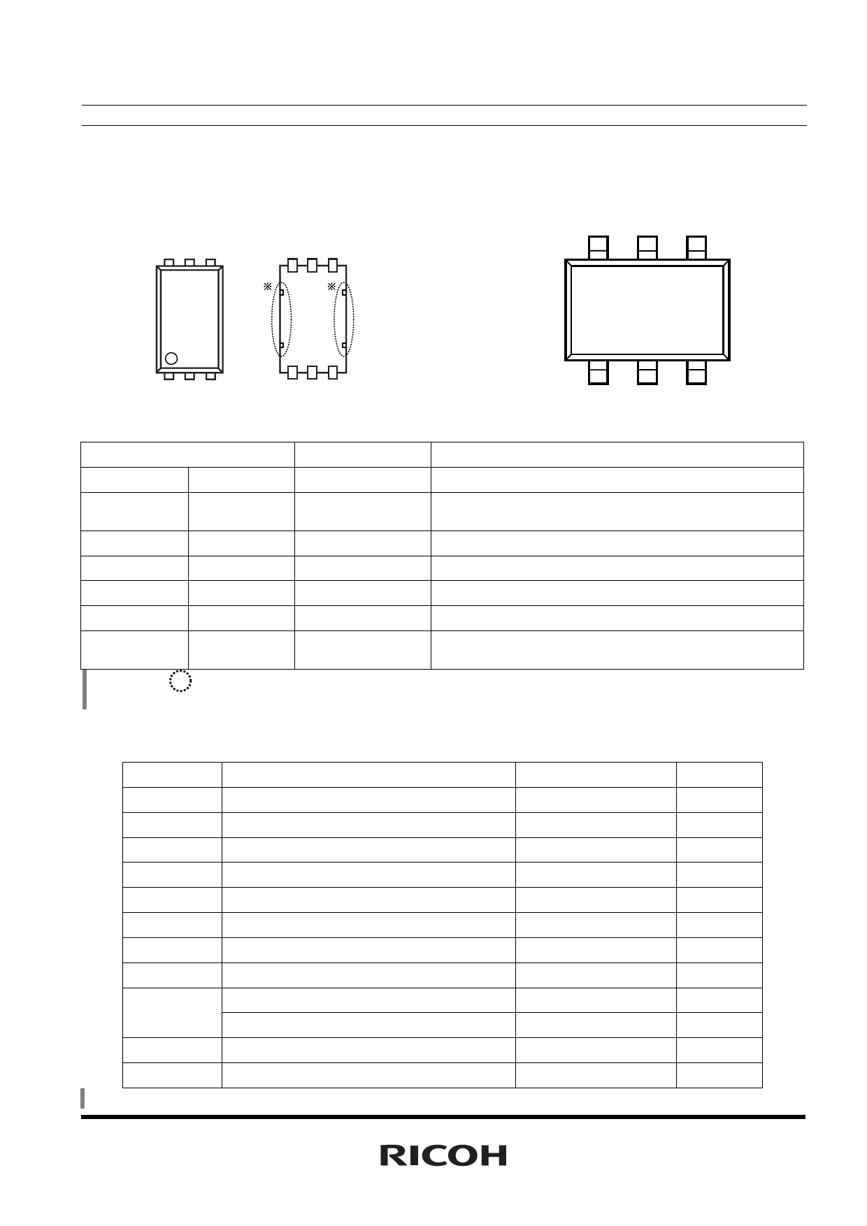
PIN CONFIGURATIONS
Top View
654
SON-6
Bottom View
456
SOT-23-6W
6
5
4
EXT GND VIN
(MARK SIDE)
DELAY AMPOUT/CE VFB
123
321
PIN DESCRIPTIONS
1
2
3
Pin No
Symbol
Pin Description
SON6
SOT23-6W
1
1
DELAY
Pin for External Capacitor
(for Setting Output Delay of Protection)
2
5
GND
Ground Pin
3
6
EXT
External FET Drive Pin (CMOS Output)
4
4
VIN
Power Supply Pin
5
3
VFB
Feedback Pin for monitoring Output Voltage
6
2
AMPOUT or CE
Amplifier Output Pin(A/C Version) or
Chip Enable Pin(B/D Version, Active at "H")
* Tab in the parts have GND level. (They are connected to the reverse side of this IC.)
Do not connect to other wires or land patterns.
ABSOLUTE MAXIMUM RATINGS
Symbol
Item
Rating
VIN
VIN Pin Voltage
6.5
VEXT
EXT Pin Output Voltage
−0.3 ~ VIN+0.3
VDLY
DELAY Pin Voltage
−0.3 ~ VIN+0.3
VAMP
AMPOUT Pin Voltage
−0.3 ~ VIN+0.3
VCE
CE Pin Input Voltage
−0.3 ~ VIN+0.3
VFB
VFB Pin Voltage
−0.3 ~ VIN+0.3
IAMP
AMPOUT Pin Current
±10
IEXT
EXT Pin Inductor Drive Output Current
±50
Power Dissipation (SOT-23-6W)*
430
PD
Power Dissipation (SON-6)*
500
Topt
Operating Temperature Range
−40 ~ +85
Tstg
Storage Temperature Range
−55 ~ +125
* ) For Power Dissipation, please refer to PACKAGE INFORMATION to be described.
Unit
V
V
V
V
V
V
mA
mA
mW
°C
°C
3
Share Link: 