AD7450BRM 查看數據表(PDF) - Analog Devices
零件编号
产品描述 (功能)
比赛名单
AD7450BRM Datasheet PDF : 24 Pages
| |||
PRELIMINARY TECHNICAL DATA
AD7450
PIN FUNCTION DESCRIPTION
Pin No. Pin Mnemonic
1
VREF
2
VIN+
3
VIN-
4
GND
5
CS
6
SDATA
7
SCLK
8
VDD
Function
Reference Input for the AD7450. An external reference must be applied to this input. For a
5 V power supply, the reference is 2.5 V (±1%) and for a 3 V power supply, the reference is
1.25 V (±1%) for specified performance. This pin should be decoupled to GND with a
capacitor of at least 0.1µF. See the ‘Reference Section’ for more details.
Positive Terminal for Differential Analog Input.
Negative Terminal for Differential Analog Input.
Analog Ground. Ground reference point for all circuitry on the AD7450. All analog input
signals and any external reference signal should be referred to this GND voltage.
Chip Select. Active low logic input. This input provides the dual function of initiating a
conversion on the AD7450 and framing the serial data transfer.
Serial Data. Logic Output. The conversion result from the AD7450 is provided on this
output as a serial data stream. The bits are clocked out on the falling edge of the SCLK
input. The data stream consists of four leading zeros followed by the 12 bits of conversion
data which are provided MSB first. The output coding is two’s complement.
Serial Clock. Logic input. SCLK provides the serial clock for accessing data from the part.
This clock input is also used as the clock source for the AD7450's conversion process.
Power Supply Input. VDD is 3 V (±10%) or 5 V (±5%). This supply should be decoupled to
GND with a 0.1µF Capacitor and a 10µF Tantalum Capacitor.
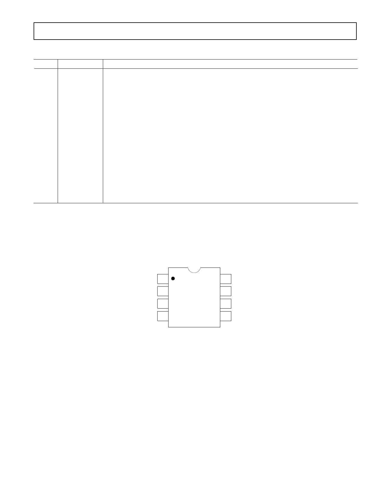
PIN CONFIGURATION SOIC and µSOIC
VREF 1
VIN + 2
VIN - 3
GND 4
AD7450
TOP VIEW
(Not to Scale)
8 VDD
7 SCLK
6 S DATA
5 CS
REV. PrJ
–5–
Share Link: 