MX651P 查看數據表(PDF) - MX-COM Inc
零件编号
产品描述 (功能)
比赛名单
MX651P Datasheet PDF : 13 Pages
| |||
Telephone SPM and Anti Fraud Tone Processor
5
MX651 - PRELIMINARY INFORMATION
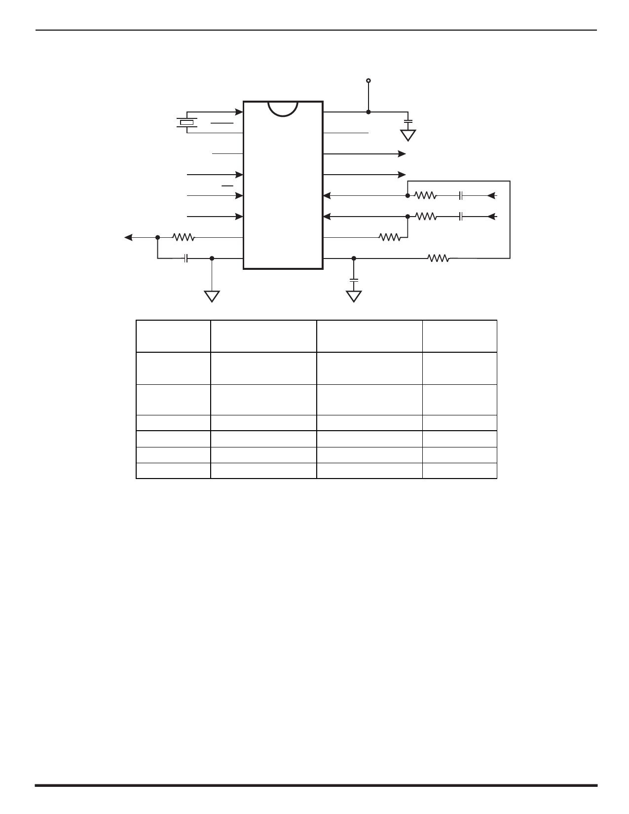
3. External Components
VDD
XTAL
XTAL
N/C
CLKIN
RX/TX
NRZ DATA
TXOUT
R5
VSS
C5
1
16
2
15
3
14
4
13
MX651
5
12
6
11
7
10
8
9
VDD
N/C
DETECT12
DETECT18
POSIN
NEGIN
AMPOUT
VBIAS
R2
C3
C4
C2
R3
C1
R1
R4
R1, R3
R2, R4
C1, C2
C3, C4
R5
C5
XTAL
See Note 1
See Note 1
See Note 1
See Note 2
1.1MΩ @ 3.3V
1.0MΩ @ 5.0V
270kΩ @ 3.3V
330kΩ @ 5.0V
33pF @ 3.3V
68pF @ 5.0V
0.1µF
51kΩ
100pF
3.579545MHz
±1%
±1%
±1%
±1%
±10%
±10%
±20%
±1%
±10%
Figure 2: Recommended External Components
External Components Notes
1. The device sensitivity is proportional to the power supply (VDD) voltage. The input gain must compensate for this and
also prevent input circuitry saturation. It is recommended that amplifier components (R1 to R4, C1 and C2) be used to
set the gain between -10dB (if VDD is 5.0V) and -13dB (if VDD is 3.3V).
2. For best results, a crystal oscillator design should drive the clock inverter input with signal levels of at least 40% of
VDD, peak-to-peak. Tuning fork type crystals generally cannot meet this requirement. To obtain crystal oscillator
design assistance, consult your crystal manufacturer
© 1997 MX•COM Inc.
www.mxcom.com Tele: 800 638-5577 910 744-5050 Fax: 910 744-5054
Doc. # 20480137.003
4800 Bethania Station Road, Winston-Salem, NC 27105-1201 USA All trademarks and service marks are held by their respective companies.
Share Link: 