MX105AP 查看數據表(PDF) - MX-COM Inc
零件编号
产品描述 (功能)
比赛名单
MX105AP Datasheet PDF : 15 Pages
| |||
Tone Detector
12
MX105A PRELIMINARY INFORMATION
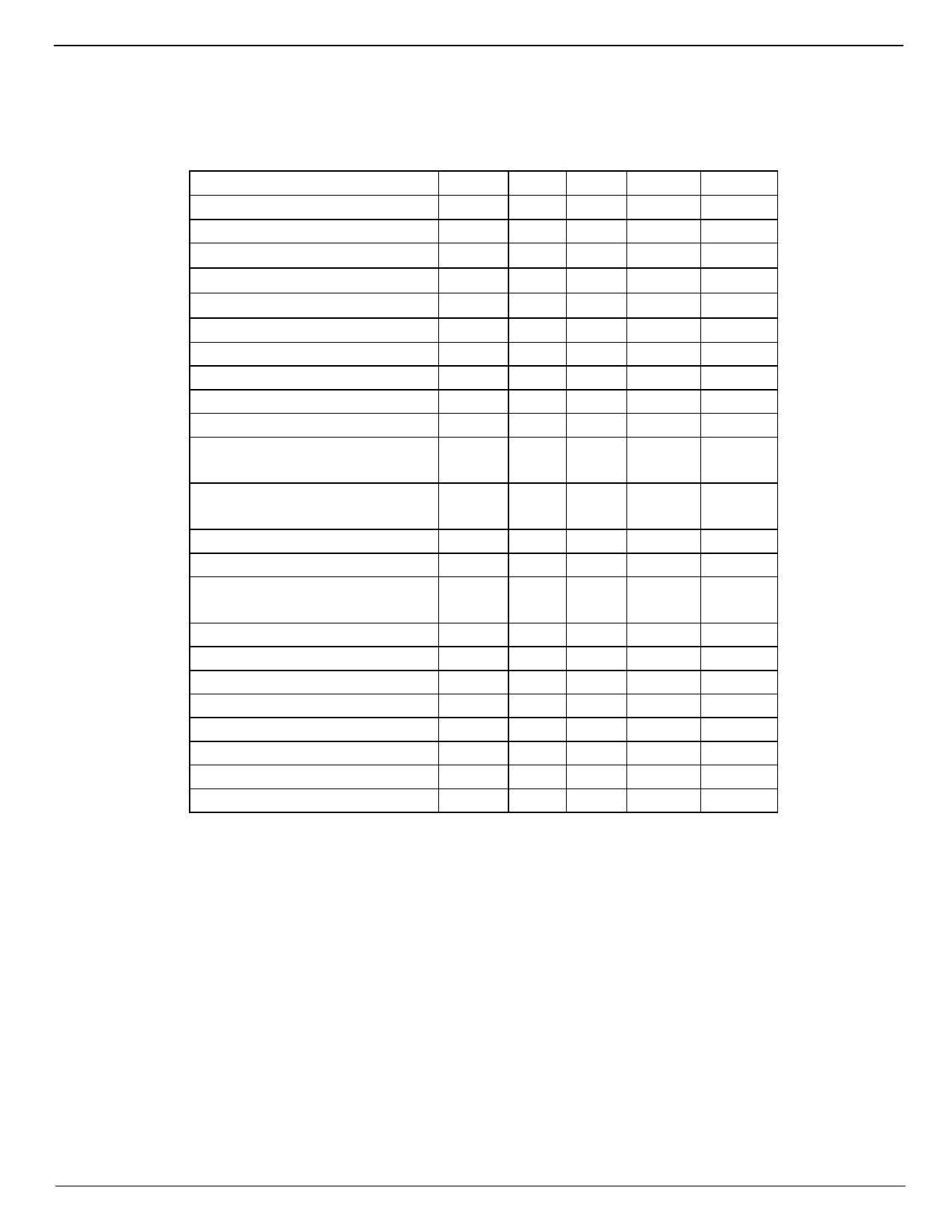
6.1.3 Operating Characteristics
For the following conditions unless otherwise specified:
VDD = 5.0 V @ TAMB = 25°C
Load resistance on decoder output = 20kΩ.
Static Parameters
IDD
Amplifier Input Impedance
Digital Output Impedance
Analog Output Impedance
Dynamic Parameters
Input Signal
Frequency
Lowest Must Detect Level
Highest Will Not Detect Level
Highest Will Not Detect f0/2
Highest Will Not Detect 5(f0)
VCO
Frequency
Frequency Stability
BW Limiter
BW Range
Amplifier
Open Loop Gain
GBWP
Closed Loop Gain
Detect Commutating Filter
Sensitivity (VTH)
Notes
1
1
1, 2
1, 2
3
1
Min.
160
40
120
2
Typ. Max. Units
1.0
mA
200
kΩ
500 1000
Ω
1000 1200
Ω
20,000
Hz
30
mVRMS
20
mVRMS
30
dB
790
mVRMS
20
dB
250
mVRMS
100
5000
120,000
Hz
ppm/°C
ppm/V
10
%f0
60
dB
1.0
MHz
0
dB
25
mVRMS
Operating Characteristics Notes:
1. Multiply by VDD /5V for other supply values.
2. The reference level is VTH. The following formula converts dB to mVRMS.
mVRMS
=
(dB/20)
10
×
VTH
3. Observing pins 13, 14, or 15 (DW/J package) will cause a frequency shift due to additional loading. If tuning center
frequency by observing oscillator, design in a buffer amplifier between pin 15 and probe/calibration point and tune with
no input signal. Otherwise, tune by observing detect output band edges while sweeping input signal. VCO center
frequency is 6(f0) at pin 15 while it is 3(f0) at pins 13 and 14.
© 1997 MX•COM, INC.
www.mxcom.com Tele: 800 638 5577 910 744 5050 Fax: 910 744 5054
Doc.# 20480133.003
4800 Bethania Station Road, Winston-Salem, NC 27105-1201 USA
All trademarks and service marks are held by their respective companies.
Share Link: 