74ACT652 查看數據表(PDF) - Fairchild Semiconductor
零件编号
产品描述 (功能)
比赛名单
74ACT652 Datasheet PDF : 8 Pages
| |||
Function Table
Inputs
Inputs/Outputs (Note 1)
Operating Mode
OEAB OEBA CPAB CPBA SAB SBA A0 thru A7 B0 thru B7
L
L
H
H
H or L H or L
X
X
X Input
X
Input
Isolation
Store A and B Data
X
H
H or L
X
X Input
Not Specified Store A, Hold B
H
L
H
X
H or L
X
X
X Input
Output
X Not Specified Input
Store A in Both Registers
Hold A, Store B
L
L X
X Output
Input
Store B in Both Registers
L
L
X
X
X
L Output
Input
Real-Time B Data to A Bus
L
L
X
H or L
X
H
Store B Data to A Bus
H
H
X
X
L
X Input
Output
Real-Time A Data to B Bus
H
H
H or L
X
H
X
Stored A Data to B Bus
H
L
H or L H or L
H
H Output
Output
Stored A Data to B Bus and
Stored B Data to A Bus
H = HIGH Voltage Level
L = LOW Voltage Level
X = Immaterial
= LOW-to-HIGH Clock Transition
Note 1: The data output functions may be enabled or disabled by various signals at OEAB or OEBA inputs. Data input functions are always enabled, i.e.,
data at the bus pins will be stored on every LOW-to-HIGH transition on the clock inputs.
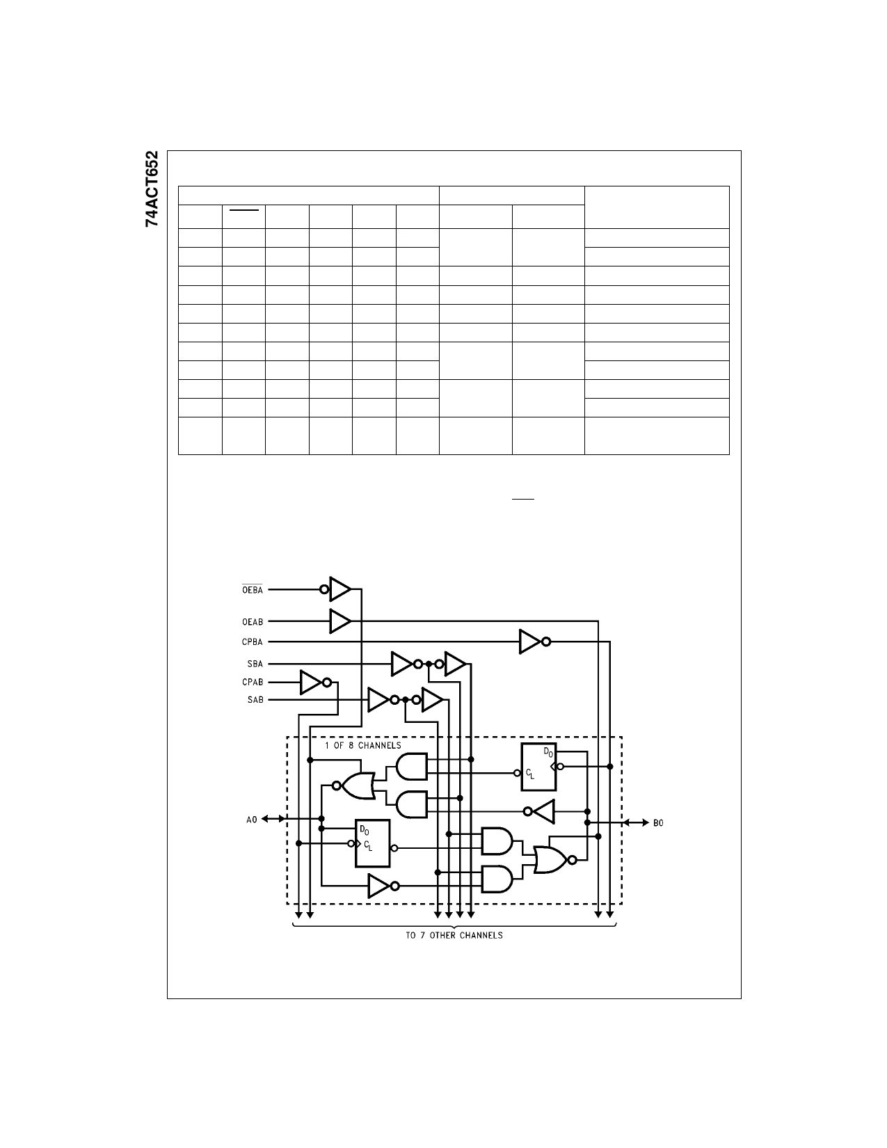
Logic Diagram
Please note that this diagram is provided only for the understanding of logic operations and should not be used to estimate propagation delays.
www.fairchildsemi.com
2
Share Link: 