VP301 查看數據表(PDF) - SANYO -> Panasonic
零件编号
产品描述 (功能)
比赛名单
VP301 Datasheet PDF : 6 Pages
| |||
VP301
Thermal Design
During operation, the transistor junction temperature must remain under 150°C, the maximum junction temperature
(Tjmax) for the VP301. The following section presents thermal design data and a thermal design example for the VP301.
Thermal Design for the VP301
The heat generated by the transistors in a video pack varies with the frequency, and also varies between the transistors in
the video pack themselves. Here, thermal design consists of selecting a heat sink such that transistor junction
temperatures in the worst case do not exceed 150°C.
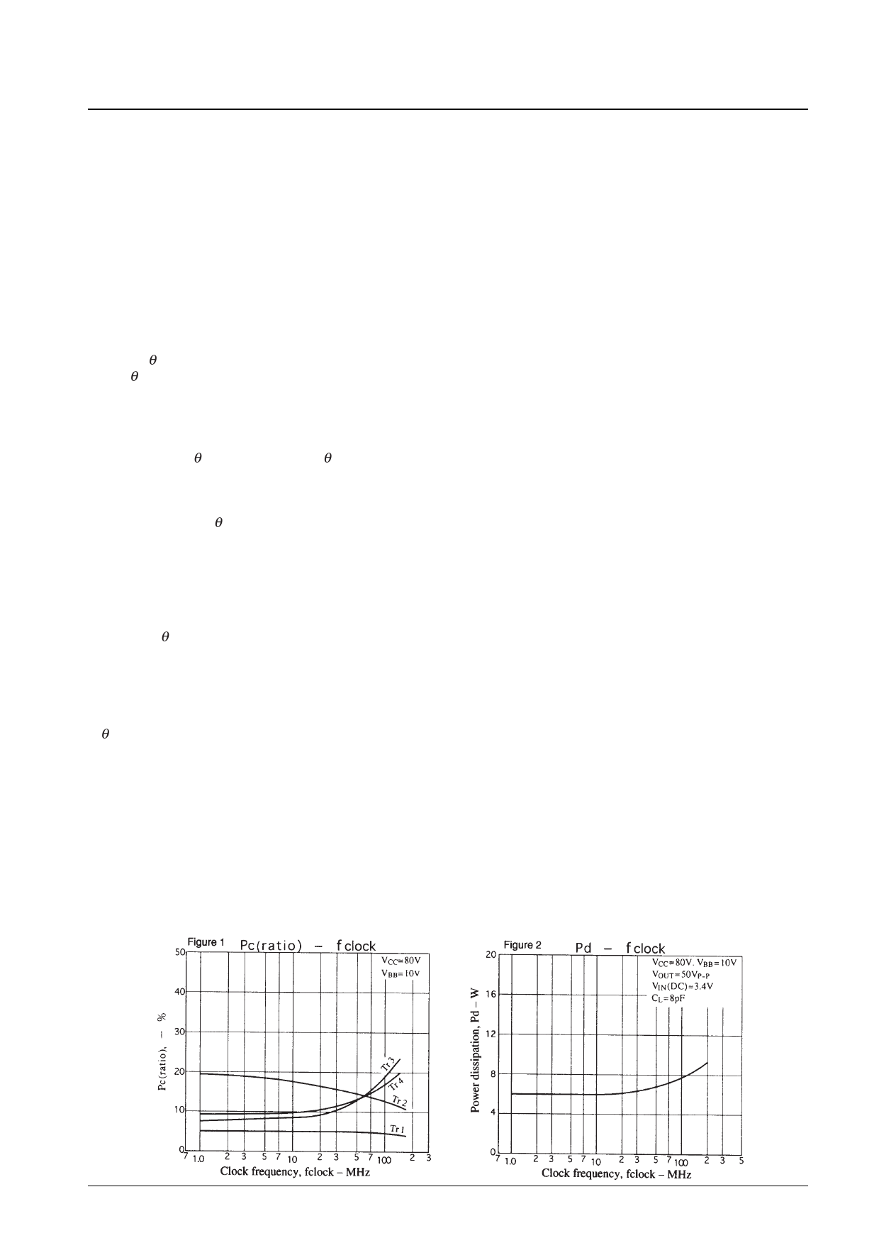
Taking the upper limit of the operating frequency, 150 MHz (clock) as a representative usage of the VP301, we consider
thermal design at this frequency. From Figure 1 we can see that transistor 3 (Tr3 in the SEPP stage) generates the largest
amount of heat, and that the loss (heat generation) in this transistor is about 22% of the total loss. The chip temperature of
each transistor is determined using the following formula.
Tj (Tri) = θj-c (Tri) × PC (Tri) + ∆Tc + Ta [°C] ...........................................Formula (1)
θj-c(Tri): Thermal resistance of an individual transistor*
Pc(Tri): Loss for an individual transistor
∆Tc: Case temperature rise
Ta: Ambient temperature (chassis internal temperature)
* For the VP301, θj-c (Tr1) = 40°C/W, θj-c (Tr2 to Tr4) = 25°C/W...........(a)
Sample Calculation
Thermal resistance, θh, for a heat sink for use at VCC = 80 V, VBB = 10 V, VO = 50 Vp-p, f = 150 MHz (clock) at
temperatures up to 60°C.
Considering figures 1 and 2, we focus on transistor 3 and determine the temperature.
The loss in transistor 3, PC(Tr3), can be estimated using the value of Pd(total) from Figure 2 to be:
PC (Tr3) = Pd (total) f = 150 MHz × PCratio (Tr3) = 8.3 × 0.22 ......................Formula (2)
≈ 1.83 [W]
From formula (1) and (a) the temperature rise for the transistor, ∆Tj(Tr3) can be calculated to be:
∆Tj (Tr3) = θj-c (Tr3) × PC (Tr3) = 25 × 1.83..............................................Formula (3)
= 45.75 [°C]
Since Tc(max) = 100°C and Tj(max) = 150°C = ∆Tj + Tc(max),
it suffices to determine a thermal resistance for the heat sink so that Tc(max) does not exceed 100°C.
Assuming operation at an ambient temperature of Ta = 60°C, the allowable case temperature rise will be: ∆Tc = 100 – 60
= 40°C. Therefore,
∴θh = ∆Tc ÷ Pd (total) f = 150 MHz = 40 ÷ 8.3..............................................Formula (4)
And this is: = 4.8[°C/W]
Note: The above calculation assumes 100% operation at the clock frequency. However, since CRT operation also
includes blanking periods, clock operation can be expected to be about 80% of the time. Since video packs are
operated at close to the cutoff state during blanking periods, the loss during this period can be assumed to be zero,
and the total loss, Pd(total), will be:
Pd (total) f = 150 MHz = Pd (total) f = 150 MHz × 0.8 = 8.3 × 0.8
= 6.64 [W]
Thus the heat sink can be made smaller than the one calculated above. We recommend performing a full thermal designs
based on the actual operating conditions.
No. 5429-5/6
Share Link: 