G525A1 查看數據表(PDF) - Global Mixed-mode Technology Inc
零件编号
产品描述 (功能)
比赛名单
G525A1 Datasheet PDF : 8 Pages
| |||
Global Mixed-mode Technology Inc.
G525A
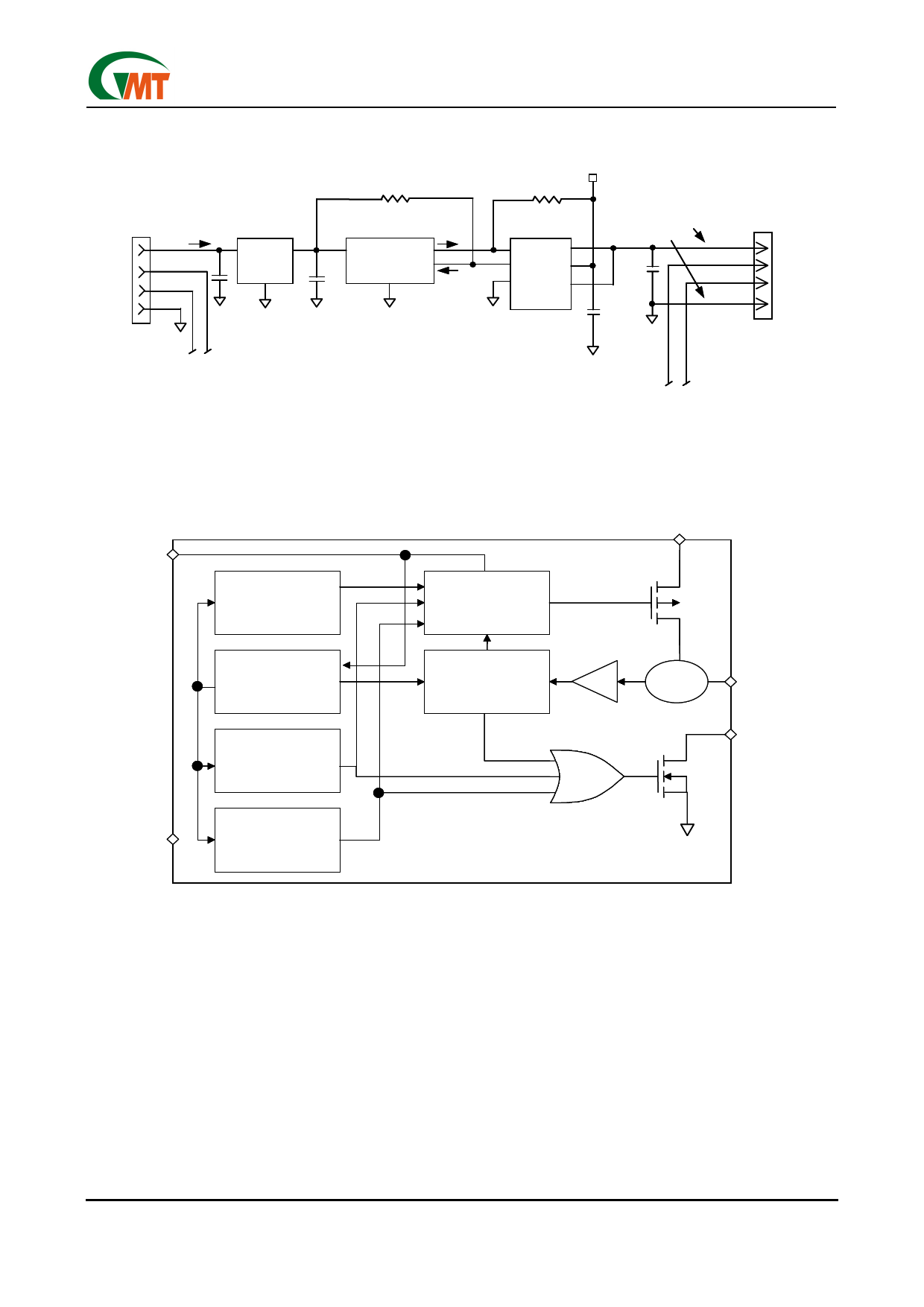
Typical Applications
VCC
5.0V
Upstream
VBUS
100mA max.
VBUS
D+ 1µF
D-
GND
G912
IN OUT
GND
10k
3.3V USB Controller
VIN ON/OFF
1 µF OVERCURRENT
GND
100k
G525A
EN OUT
FLG IN
GND OUT
NC NC
Ferrite
Beads
+
150 µF
VBUS
D+
D-
GND
USB
Port
Data
0.1 µF
Data
Single-Port Self-Powered USB Hub Application
Function Block Diagrams
EN
Clock
IN
Gate Control
BandGap
Reference
UVLO
Overcurrent
Limiting
CMP
Current
Sense
OUT
FLG
GND
Thermal Sense
Functional Description
The G525A1 and G525A2 are high-side 1-channel
switches with active-high and active-low enable inputs,
respectively. Fault conditions turn off or inhibit turn-on
of the output transistors and activate the open-drain
error flag transistors to pull FLG pin to ground.
Input and Output
IN (input) is the power supply connection to the logic
circuitry and the source of the output MOSFET. OUT
(output) is the drain of the output MOSFET. In a typical
application, current flows through the switch from IN to
OUT toward the load. Both OUT pins must be
connected together to the load.
The output MOSFET and driving circuit are also de-
signed to allow the MOSFET drain to be externally
forced to a higher voltage than the source (VOUT > VIN)
when the switch is off. In this situation, the G525A
avoids undesirable drain-to-body diode current flow by
connecting the body to the most positive voltage. If
VOUT >VIN when switch is enabled, current will flow
from VOUT to VIN.
Thermal Shutdown
Thermal shutdown protects G525A from excessive
power dissipation. If the die temperature exceeds
135°C, the MOSFETS switch is shut off and a fault
flag is activated. 10°C of hystersis prevents the switch
Ver: 1.2
Nov 11, 2002
TEL: 886-3-5788833
http://www.gmt.com.tw
5
Share Link: 