G525A 查看數據表(PDF) - Global Mixed-mode Technology Inc
零件编号
产品描述 (功能)
比赛名单
G525A Datasheet PDF : 8 Pages
| |||
Global Mixed-mode Technology Inc.
G525A
from turning on until the die temperature drops to
125°C. Thermal shutdown circuit functions only when
the switch is enabled.
Undervoltage Lockout
UVLO (undervoltage lockout) prevents the output
MOSFET from turning on until IN (input voltage) ex-
ceeds 2.5V typically. After the switch turns on, if the
voltage drops below 2.3V typically, UVLO shuts off the
output MOSFET and signals the fault flag. UVLO de-
tection functions only when the switch is enabled.
Current Sensing and Limiting
The current limit threshold is preset internally. The
preset level prevents damage to the output MOSFET
and external load but allows a minimum current of
0.5A through the output MOSFET.
A current sense circuit senses the output current of
MOSFET switch. If output current exceeds the current
limit threshold, the output MOSFET switch is shut off
and a fault flag is pulled low. The reaction to an over-
current is measured with the following scenarios:
Switch Enabled into Heavy Load
If the switch is powered on or enabled into a heavy
load or short-circuit, the switch immediately goes into
a constant-current mode, reducing the output voltage.
The fault flag goes low until the load is reduced or
thermal shutdown occurs. See the "Enable into Short
Circuit" graph.
Fault Flag
FLG is a 2-channel, open-drain MOSFET output. The
fault-flag is active (low) for one or more of the follow-
ing conditions: current limiting, undervoltage, or ther-
mal shutdown. The flag output MOSFET is capable of
sinking a 10mA load to typically 100mV above ground.
Applications Information
Supply filtering
A 0.1µF to 1µF bypass capacitor from IN to GND, lo-
cated near the G525A, is strongly recommended to
control supply transients. Without a bypass capacitor,
an output short may cause sufficient ringing on the
input (from supply lead inductance) to damage internal
control circuitry.
Input transients must not exceed the absolute maxi-
mum supply voltage (VIN max = 6V) even for a short du-
ration.
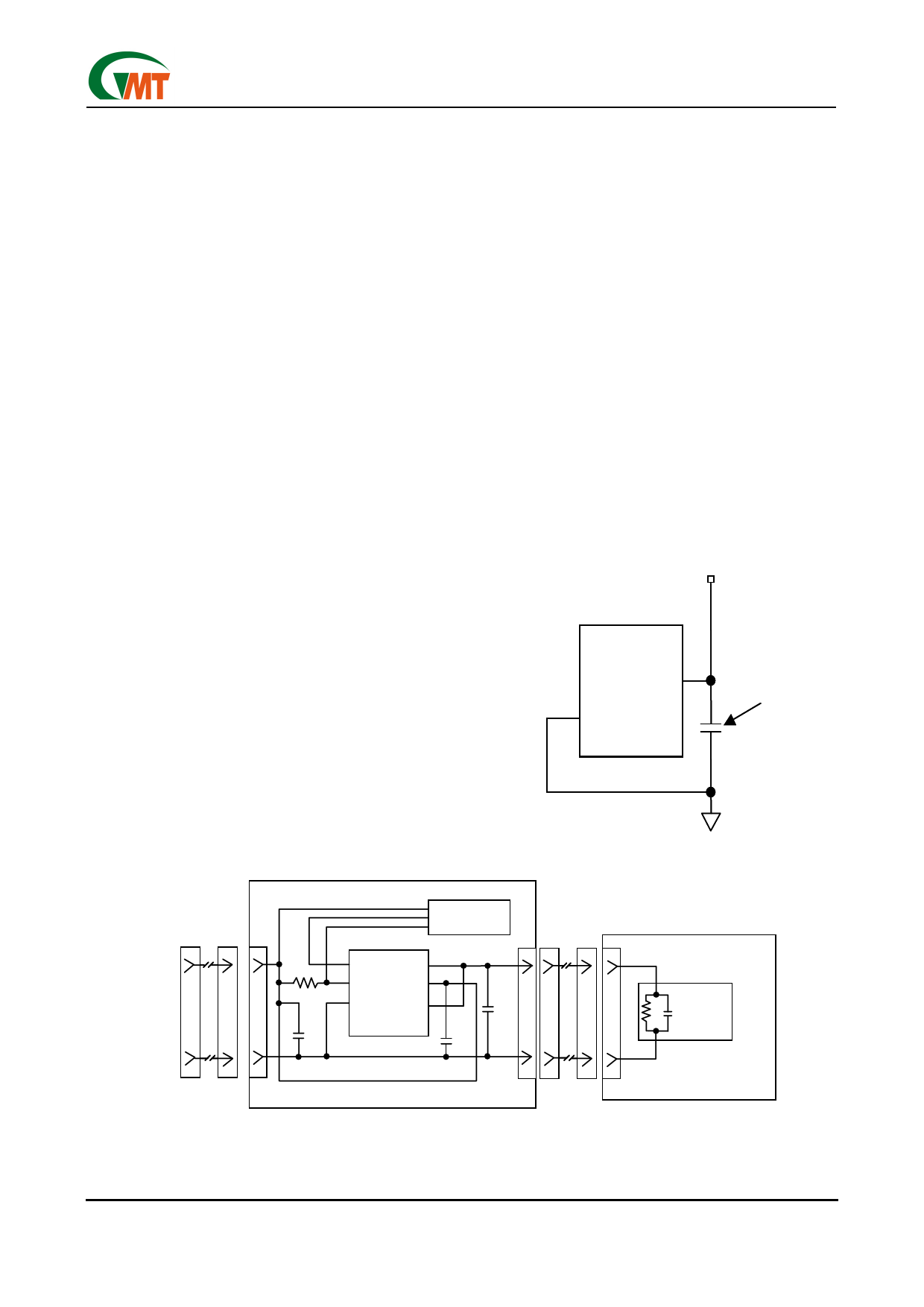
Figure 1. Supply Bypassing
3.0V to 5.5V
G525A
1 EN
OUT 8
Heavy Load Applied to Enabled Switch
When a heavy load is applied, a large current may
flow from the switch. The current limit circuit may shut
the switch off briefly, then fold back into con-
stant-current mode. In that case, the fault flag falls
until the load is reduced. See the “Short Applied to
Output” graph and the "Ramped Load to Enable De-
vice" graph.
2 FLG
3 GND
4 NC
IN 7
OUT 6
NC 5
0.1 µF to 1 µF
VBUS
USB Host
GND
Cable
Ver: 1.2
Nov 11, 2002
USB
Controller
G525A
1
8
2
EN
FLG
3 GND
4.7
µF
4 NC
OUT
IN
7
OUT 6
NC 5
CBULK
0.1 µF
Bus Powered Hub
Cable
Figure 2. Soft Start
Capacitive
Load
Downstream USB Device
TEL: 886-3-5788833
http://www.gmt.com.tw
6
Share Link: 