RF2681 查看數據表(PDF) - RF Micro Devices
零件编号
产品描述 (功能)
比赛名单
RF2681 Datasheet PDF : 8 Pages
| |||
Preliminary
RF2681
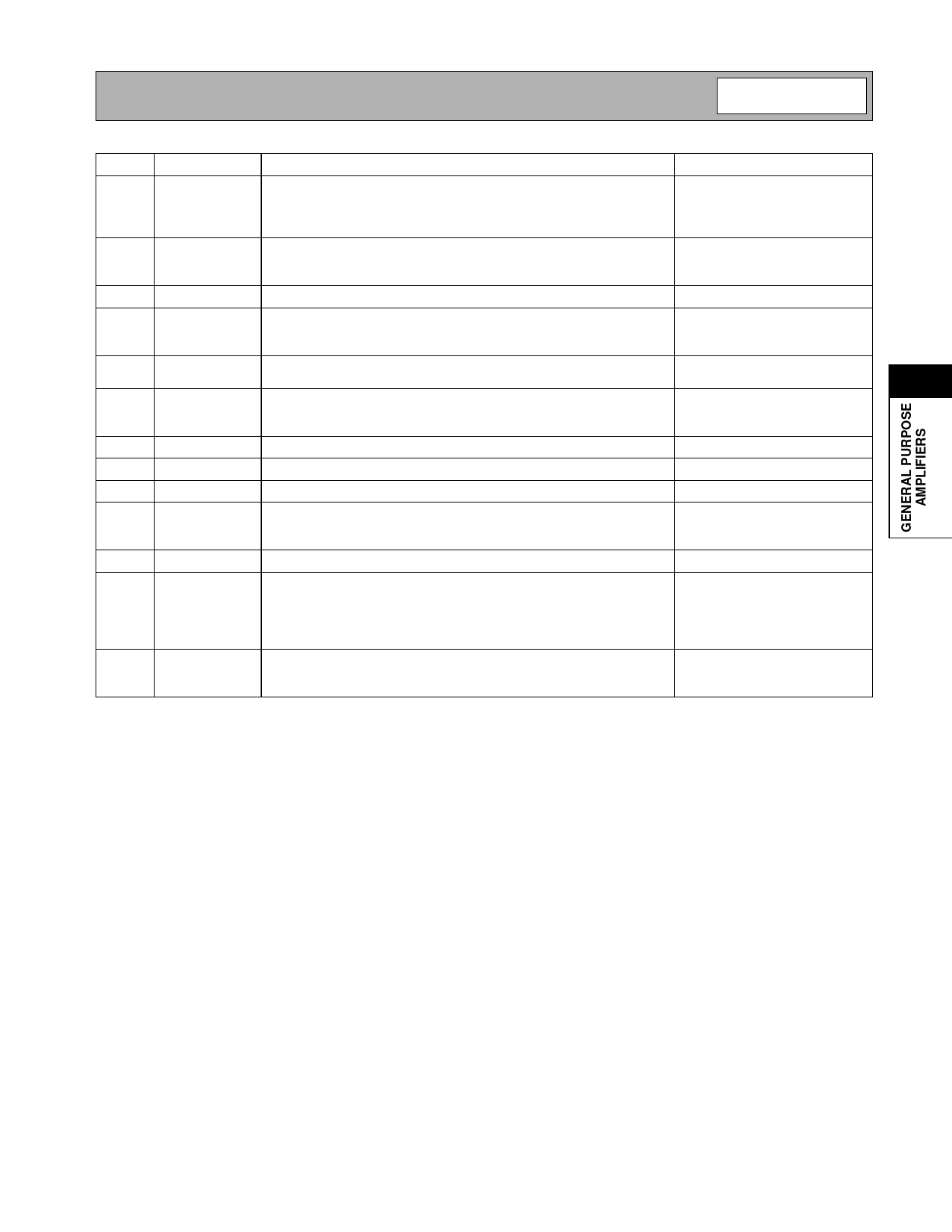
Pin Function Description
Interface Schematic
1
VCC1
DC supply for internal bias circuitry. This pin should be tied to VCC, and
must be bypassed with an RF capacitor. The trace length between the
pin and the bypass capacitor should be minimized. The ground side of
the capacitor should connect immediately to the ground plane.
2
VREG
DC supply for internal bias circuitry. This pin should be tied to a 2.7V
supply for proper operation. Increasing this voltage above 2.7V will
result in increased current drain and is not recommended.
3
VCC2
Same as pin 1.
4
PD
Power down pin. This pin should be brought below 1V for proper opera-
tion. The device is turned off when the voltage on this pin increases
above 2V.
5
NC
This pin is not internally connected, but should be grounded, if possi-
ble, to improve RF isolation. Please refer to the evaluation board layout.
4
6
RF IN
RF input pin. This pin requires external matching components, and is
DC-coupled. Please refer to the applications schematic for recom-
mended matching components.
7
GND
Ground
8
GND
Ground
9
GND
Ground
10
RF OUT RF output pin. This pin requires an external matching network. VCC is
provided through an inductor of that network. Please refer to the appli-
cations schematic for recommended matching components.
11
NC
Same as pin 5.
12
GC
Gain control pin. This pin allows the gain of the amplifier to be varied in
a continuous “analog” fashion. With an applied voltage of 0.2V or less,
the amplifier exhibits the minimum gain. In the region between 0.2V
and 2.25V, the amplifier gain in dB depends on the voltage in a roughly
linear manner. Above 2.25V, the amplifier gain is set for maximum.
Pkg
Gnd
GND
Ground connection for the device “die flag”. The backside of the pack-
age should be soldered to a top side ground pad which is connected to
the PC board ground plane through multiple vias.
Rev A1 010824
4-45
Share Link: 