XA-G49(2000) 查看數據表(PDF) - Philips Electronics
零件编号
产品描述 (功能)
比赛名单
XA-G49
(Rev.:2000)
(Rev.:2000)
Philips Electronics

XA-G49 Datasheet PDF : 42 Pages
| |||
Philips Semiconductors
XA 16-bit microcontroller family
64K Flash/2K RAM, watchdog, 2 UARTs
Preliminary specification
XA-G49
GENERAL DESCRIPTION
The XA-G49 is a member of Philips’ 80C51 XA (eXtended
Architecture) family of high performance 16-bit single-chip
microcontrollers.
The XA-G49 contains 64k bytes of Flash program memory, and
provides three general purpose timers/counters, a watchdog timer,
dual UARTs, and four general purpose I/O ports with programmable
output configurations.
A default serial loader program in the Boot ROM allows In-System
Programming (ISP) of the Flash memory without the need for a
loader in the Flash code. User programs may erase and reprogram
the Flash memory at will through the use of standard routines
contained in the Boot ROM (In-Application Programming).
FEATURES
• 4.5V to 5.5V operation. For low voltage operation, consult factory.
• 64K bytes of on-chip Flash program memory with In-System
Programming capability
• Five Flash blocks = two 8k byte blocks and three 16k byte blocks
• Nearly identical to XA-G3, except for double the program and
RAM memories
• Single supply voltage In-System Programming (ISP) of the Flash
memory (VPP = VDD, or VPP = 12V if desired)
• Boot ROM contains low level Flash programming routines for
In-Application Programming and a default serial loader using the
UART
• 2048 bytes of on-chip data RAM
• Supports off-chip program and data addressing up to 1 megabyte
(20 address lines)
• Three standard counter/timers with enhanced features (same as
XA-G3 T0, T1, and T2). All timers have a toggle output capability
• Watchdog timer
• Two enhanced UARTs with independent baud rates
• Seven software interrupts
• Four 8-bit I/O ports, with 4 programmable output configurations for
each pin
• 30 MHz operating frequency at 5V
• Power saving operating modes: Idle and Power-Down.
Wake-Up from power-down via an external interrupt is supported.
• 44-pin PLCC and 44-pin LQFP packages
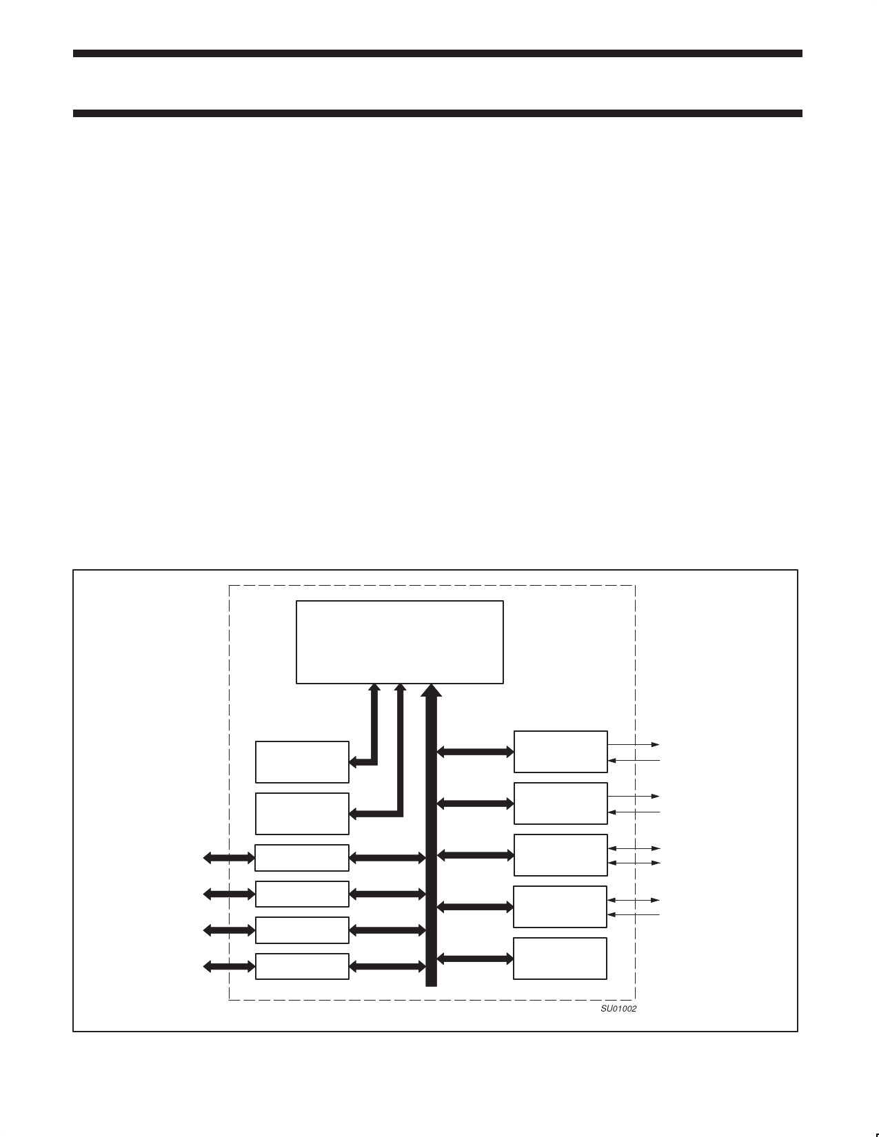
BLOCK DIAGRAM
XA CPU Core
Program
Memory
Bus
64K Bytes
FLASH
2048 Bytes
Static RAM
Data
Bus
Port 0
Port 1
Port 2
Port 3
SFR
bus
UART 0
UART 1
Timer 0, 1
Timer 2
Watchdog
Timer
SU01002
2000 Apr 03
2
Share Link: