BQ24075RGTR 查看數據表(PDF) - Teccor Electronics
零件编号
产品描述 (功能)
比赛名单
BQ24075RGTR Datasheet PDF : 53 Pages
| |||
www.ti.com
bq24072, bq24073, bq24074, bq24075, bq24079
SLUS810L – SEPTEMBER 2008 – REVISED JUNE 2018
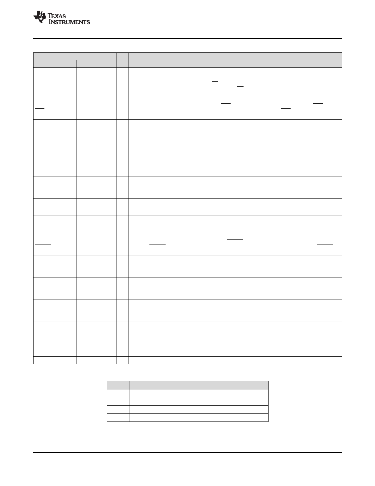
NAME
BAT
CE
CHG
EN1
EN2
ILIM
IN
ISET
ITERM
OUT
PGOOD
SYSOFF
TD
Thermal
Pad
TMR
TS
VSS
PIN
'72, '73 '74
2, 3
2, 3
4
4
9
9
6
6
5
5
12
12
13
13
16
16
–
15
10, 11 10, 11
7
7
–
–
15
–
—
—
14
14
1
1
8
8
'75, '79
2, 3
4
9
6
5
12
13
16
–
10, 11
7
15
–
—
14
1
8
Pin Functions
I/O
DESCRIPTION
I/O
Charger Power Stage Output and Battery Voltage Sense Input. Connect BAT to the positive terminal of the
battery. Bypass BAT to VSS with a 4.7-μF to 47-μF ceramic capacitor.
Charge Enable Active-Low Input. Connect CE to a high logic level to disable battery charging. OUT is active
I
and battery supplement mode is still available. Connect CE to a low logic level to enable the battery charger.
CE is internally pulled down with approximately 285 kΩ. Do not leave CE unconnected to ensure proper
operation.
Open-Drain Charging Status Indication Output. CHG pulls to VSS when the battery is charging. CHG is high
O impedance when charging is complete and when charger is disabled. Connect CHG to the desired logic
voltage rail using a 1kΩ-100kΩ resistor, or use with an LED for visual indication.
I Input Current Limit Configuration Inputs. Use EN1 and EN2 control the maximum input current and enable
USB compliance. See Table 1 for the description of the operation states. EN1 and EN2 are internally pulled
I down with ≉285 kΩ. Do not leave EN1 or EN2 unconnected to ensure proper operation.
Adjustable Current Limit Programming Input. Connect a 1100-Ω to 8-kΩ resistor from ILIM to VSS to program
I the maximum input current (EN2=1, EN1=0). The input current includes the system load and the battery
charge current. Leaving ILIM unconnected disables all charging.
Input Power Connection. Connect IN to the external DC supply (AC adapter or USB port). The input operating
I
range is 4.35 V to 6.6 V (bq24072, bq24073, bq24075, and bq24079) or 4.35 V to 10.5 V (bq23074). The
input can accept voltages up to 26 V without damage but operation is suspended. Connect bypass capacitor
1 μF to 10 μF to VSS.
Fast Charge Current Programming Input. Connect a 590-Ω to 8.9-kΩ resistor from ISET to VSS to program
I/O
the fast charge current level. Charging is disabled if ISET is left unconnected. While charging, the voltage at
ISET reflects the actual charging current and can be used to monitor charge current. See Charge Current
Translator for more details.
Termination Current Programming Input. Connect a 0-Ω to 15-kΩ resistor from ITERM to VSS to program the
I termination current. Leave ITERM unconnected to set the termination current to the default 10% termination
threshold.
System Supply Output. OUT provides a regulated output when the input is below the OVP threshold and
O
above the regulation voltage. When the input is out of the operation range, OUT is connected to VBAT except
when SYSOFF is high (bq24075 and bq24079 only). Connect OUT to the system load. Bypass OUT to VSS
with a 4.7-μF to 47-μF ceramic capacitor.
Open-drain Power Good Status Indication Output. PGOOD pulls to VSS when a valid input source is
O detected. PGOOD is high-impedance when the input power is not within specified limits. Connect PGOOD to
the desired logic voltage rail using a 1-kΩ to 100-kΩ resistor, or use with an LED for visual indication.
System Enable Input. Connect SYSOFF high to turn off the FET connecting the battery to the system output.
I
When an adapter is connected, charging is also disabled. Connect SYSOFF low for normal operation.
SYSOFF is internally pulled up to VBAT through a large resistor (approximately 5 MΩ). Do not leave SYSOFF
unconnected to ensure proper operation.
Termination Disable Input. Connect TD high to disable charger termination. Connect TD to VSS to enable
I
charger termination. TD is checked during startup only and cannot be changed during operation. See the TD
section in this datasheet for a description of the behavior when termination is disabled. TD is internally pulled
down to VSS with approximately 285 kΩ. Do not leave TD unconnected to ensure proper operation.
There is an internal electrical connection between the exposed thermal pad and the VSS pin of the device.
–
The thermal pad must be connected to the same potential as the VSS pin on the printed circuit board. Do not
use the thermal pad as the primary ground input for the device. VSS pin must be connected to ground at all
times.
Timer Programming Input. TMR controls the pre-charge and fast-charge safety timers. Connect TMR to VSS
I to disable all safety timers. Connect a 18-kΩ to 72-kΩ resistor between TMR and VSS to program the timers
a desired length. Leave TMR unconnected to set the timers to the default values.
External NTC Thermistor Input. Connect the TS input to the NTC thermistor in the battery pack. TS monitors
I a 10kΩ NTC thermistor. For applications that do not use the TS function, connect a 10-kΩ fixed resistor from
TS to VSS to maintain a valid voltage level on TS.
– Ground. Connect to the thermal pad and to the ground rail of the circuit.
Table 1. EN1/EN2 Settings
EN2 EN1 MAXIMUM INPUT CURRENT INTO IN PIN
0
0 100 mA. USB100 mode
0
1 500 mA. USB500 mode
1
0 Set by an external resistor from ILIM to VSS
1
1 Standby (USB suspend mode)
Copyright © 2008–2018, Texas Instruments Incorporated
Submit Documentation Feedback
7
Product Folder Links: bq24072 bq24073 bq24074 bq24075 bq24079
Share Link: 