LT3574IMS 查看數據表(PDF) - Linear Technology
零件编号
产品描述 (功能)
比赛名单
LT3574IMS Datasheet PDF : 24 Pages
| |||
Applications Information
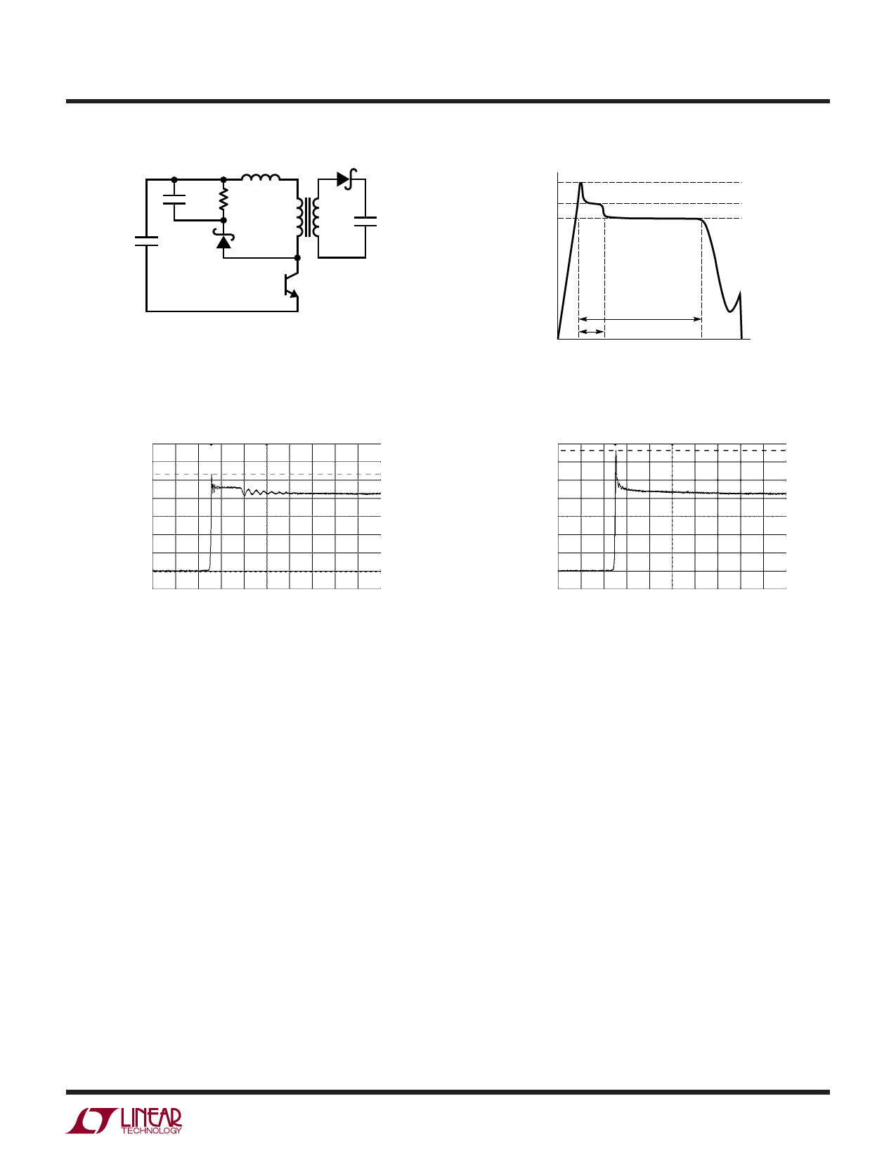
LS
C
R
D
•
•
3574 F04
Figure 4. RCD Clamp
VSW
< 60V
< 55V
< 50V
LT3574
tOFF > 350ns
tSP < 150ns
TIME
3574 F05
Figure 5. Maximum Voltages for SW Pin Flyback Waveform
10V/DIV
10V/DIV
100ns/DIV
3574 F06
Figure 6. Good Snubber Diode Limits SW Pin Voltage
100ns/DIV
3574 F07
Figure 7. Bad Snubber Diode Does Not Limit SW Pin Voltage
Secondary Leakage Inductance
In addition to the previously described effects of leakage
inductance in general, leakage inductance on the second-
ary in particular exhibits an additional phenomenon. It
forms an inductive divider on the transformer secondary
that effectively reduces the size of the primary-referred
flyback pulse used for feedback. This will increase the
output voltage target by a similar percentage. Note that
unlike leakage spike behavior, this phenomenon is load
independent. To the extent that the secondary leakage
inductance is a constant percentage of mutual inductance
(over manufacturing variations), this can be accommodated
by adjusting the RFB/RREF resistor ratio.
Winding Resistance Effects
Resistance in either the primary or secondary will reduce
overall efficiency (POUT / PIN). Good output voltage regula-
tion will be maintained independent of winding resistance
due to the boundary mode operation of the LT3574.
Bifilar Winding
A bifilar, or similar winding technique, is a good way to
minimize troublesome leakage inductances. However, re-
member that this will also increase primary-to-secondary
capacitance and limit the primary-to-secondary breakdown
voltage, so, bifilar winding is not always practical. The
Linear Technology applications group is available and
extremely qualified to assist in the selection and/or design
of the transformer.
3574f
13
Share Link: 