AQV251 查看數據表(PDF) - Panasonic Corporation
零件编号
产品描述 (功能)
比赛名单
AQV251
Panasonic Corporation

AQV251 Datasheet PDF : 4 Pages
| |||
HE 1 Form A (AQV25❍)
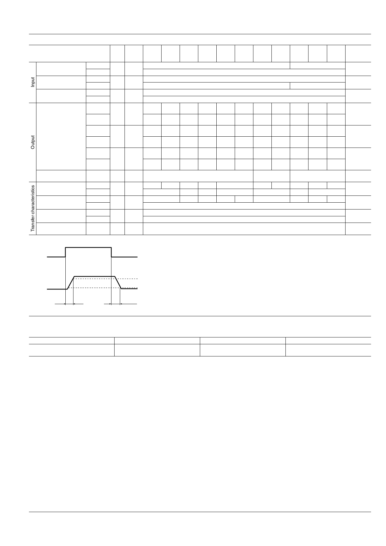
2. Electrical characteristics (Ambient temperature: 25°C 77°F)
Item
Sym-
bol
Type of
con- AQV251(A) AQV252(A) AQV255(A) AQV257(A) AQV253(A) AQV254(A) AQV259(A) AQV258(A) AQV253H(A) AQV254H(A) AQV256H(A)
nection
Condition
Typical
LED operate current
IFon
—
Maximum
0.9 mA
3 mA
1.4 mA
IL = Max.
Minimum
LED turn off current
IFoff
—
Typical
0.8 mA
0.4 mA
1.3 mA
IL = Max.
Typical
LED dropout voltage
VF
—
Maximum
1.25 V (1.14 V at IF = 5 mA)
1.5 V
IF = 50 mA
On resistance
Typical
Ron
Maximum
A
0.6 Ω 0.74 Ω 1.8 Ω
1 Ω 1.4 Ω 2.5 Ω
2.6 Ω
4Ω
5.5 Ω 12.4 Ω 85 Ω 345 Ω
8 Ω 16 Ω 200 Ω 500 Ω
5.5 Ω 12.4 Ω
8 Ω 16 Ω
20 Ω
30 Ω
IF = 5 mA
IL = Max.
Within 1 s
on time
Typical
0.3Ω 0.37 Ω 0.9 Ω 1.4 Ω 2.7 Ω 6.2 Ω 60 Ω 345 Ω 2.7 Ω 6.2 Ω 15 Ω IF = 5 mA
Ron
Maximum
B
0.5 Ω 0.7 Ω 1.25 Ω 2 Ω
4Ω
8 Ω 100 Ω 500 Ω 4 Ω
IL = Max.
8Ω
20 Ω
Within 1 s
on time
Typical
Ron
Maximum
0.15 Ω 0.18 Ω 0.45 Ω 0.7 Ω 1.4 Ω 3.1 Ω 30 Ω 160 Ω 1.4 Ω 3.1 Ω 7.5 Ω IF = 5 mA
C
0.25 Ω 0.35 Ω 0.63 Ω 1 Ω
2Ω
4 Ω 50 Ω 250 Ω 2 Ω
IL = Max.
4Ω
10 Ω
Within 1 s
on time
Off state leakage
current
Turn on time*
Maximum ILeak
Typical
Ton
Maximum
—
1 µA
1.7 ms 1.4 ms 0.9 ms 1.5 ms
—
3 ms
2 ms 3 ms
0.8 ms
2 ms
10 µA
0.6 ms 0.35 ms
1 ms
2.4 ms
4 ms
1 µA
1.8 ms 1.2 ms
3ms
IF = 0 mA
VL = Max.
IF = 5 mA
IL = Max.
Turn off time*
Typical
Toff
—
Maximum
0.07 ms
0.09 ms 0.1 ms 0.06 ms 0.05 ms
0.2 ms
0.04 ms
0.06 ms 0.05 ms 0.06 ms IF = 5 mA
IL = Max.
I/O capacitance
Typical
Ciso
—
Maximum
1.3 pF
3 pF
f = 1 MHz
VB = 0 V
Initial I/O isolation
resistance
Minimum Riso
—
1,000 MΩ
500 V DC
*Turn on/Turn off time
Input
Output
Ton
90%
10%
Toff
RECOMMENDED OPERATING CONDITIONS
Please obey the following conditions to ensure proper device operation and resetting.
Item
Symbol
Recommended value
Unit
Input LED current
IF
Standard type: 5
Reinforced insulation type: 5 to 10
mA
■ For Dimensions.
■ For Schematic and Wiring Diagrams.
■ For Cautions for Use.
■ These products are not designed for automotive use.
If you are considering to use these products for automotive applications, please contact your local Panasonic Corporation
technical representative.
For more information.
■ Continual DC bias (for AQV258❇❇, AQV259❇❇)
In cases in which a continual DC bias is applied between the input and output, the output-side MOS-FET may deteriorate
due to the voltage. Therefore, please verify operation of the actual design before using. An example of a circuit that might
undergo MOS-FET deterioration due to voltage is given below.
ASCTB143E 201201-T
Panasonic Corporation Automation Controls Business Unit industrial.panasonic.com/ac/e
Share Link: