FM24C64VN 查看數據表(PDF) - Fairchild Semiconductor
零件编号
产品描述 (功能)
比赛名单
FM24C64VN Datasheet PDF : 13 Pages
| |||
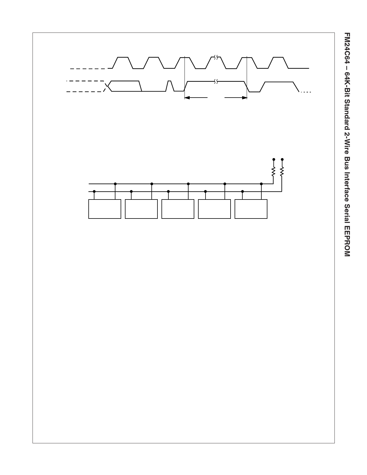
Write Cycle Timing
SCL
SDA
8th BIT
ACK
Note:
WORD n
STOP
CONDITION
tWR
START
CONDITION
The write cycle time (tWR) is the time from a valid stop condition of a write sequence to the end of the internal erase/program cycle.
Typical System Configuration
VCC
VCC
SDA
SCL
Master
Transmitter/
Receiver
Slave
Receiver
Slave
Transmitter/
Receiver
Master
Transmitter
Master
Transmitter/
Receiver
Note: Due to open drain configuration of SDA and SCL, a bus-level pull-up resistor is called for, (typical value = 4.7kΩ)
FM24C64 Rev. C
6
www.fairchildsemi.com
Share Link: 