74HC595(2004) 查看數據表(PDF) - STMicroelectronics
零件编号
产品描述 (功能)
比赛名单
74HC595 Datasheet PDF : 16 Pages
| |||
M74HC595
8 BIT SHIFT REGISTER
WITH OUTPUT LATCHES (3 STATE)
s HIGH SPEED:
fMAX = 59MHz (TYP.) at VCC = 6V
s LOW POWER DISSIPATION:
ICC = 4µA(MAX.) at TA=25°C
s HIGH NOISE IMMUNITY:
VNIH = VNIL = 28% VCC (MIN.)
s SYMMETRICAL OUTPUT IMPEDANCE:
|IOH| = IOL = 6mA (MIN.) FOR QA to QH
|IOH| = IOL = 4mA (MIN.) FOR QH’
s BALANCED PROPAGATION DELAYS:
tPLH ≅ tPHL
s WIDE OPERATING VOLTAGE RANGE:
VCC (OPR) = 2V to 6V
s PIN AND FUNCTION COMPATIBLE WITH
74 SERIES 595
DESCRIPTION
The M74HC595 is an high speed CMOS 8-BIT
SHIFT REGISTERS/OUTPUT LATCHES
(3-STATE) fabricated with silicon gate C2MOS
technology.
This device contains an 8-bit serial-in, parallel-out
shift register that feeds an 8-bit D-type storage
register. The storage register has 8 3-STATE
outputs. Separate clocks are provided for both the
shift register and the storage register.
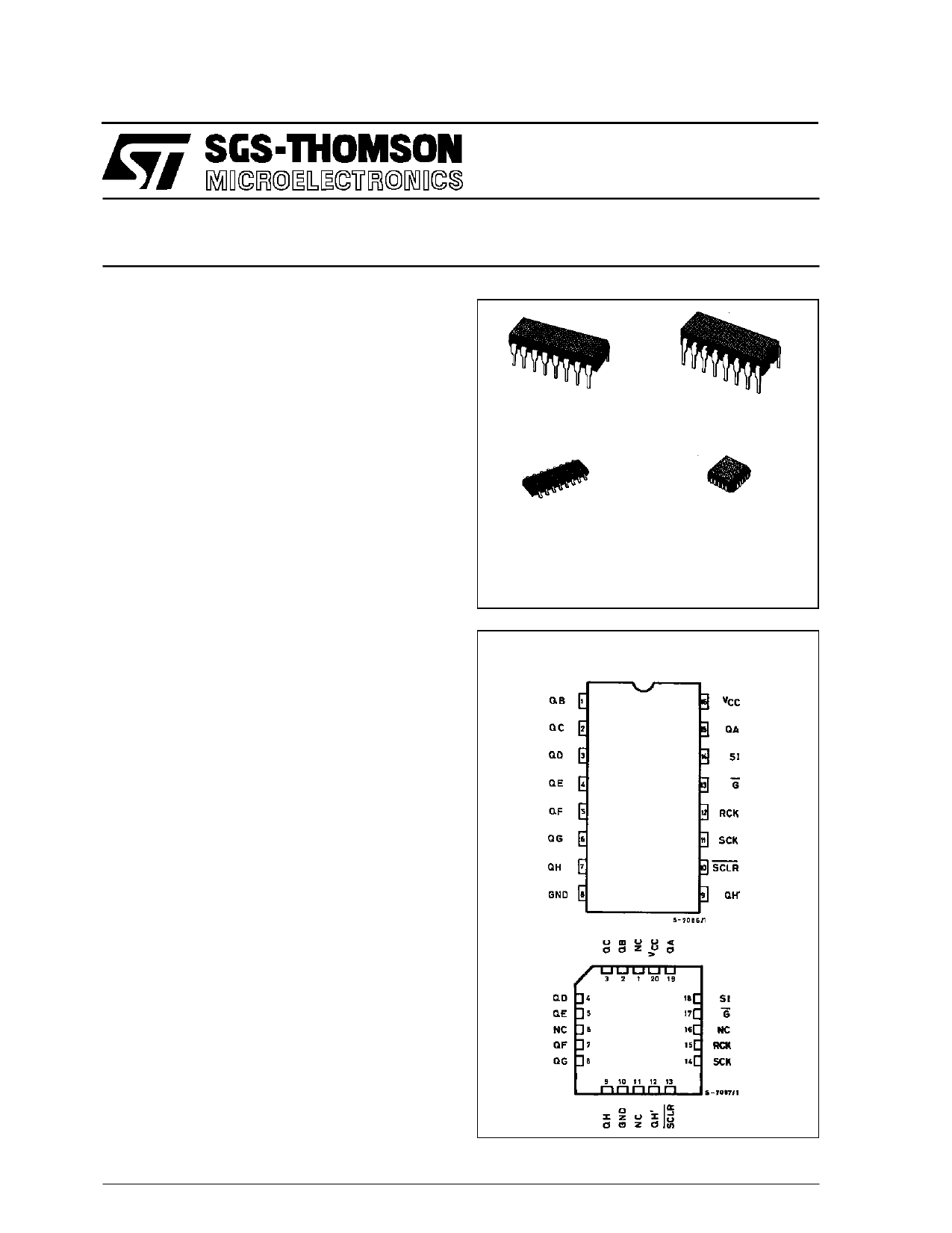
DIP
SOP
TSSOP
ORDER CODES
PACKAGE
TUBE
DIP
SOP
TSSOP
M74HC595B1R
M74HC595M1R
T&R
M74HC595RM13TR
M74HC595TTR
The shift register has a direct-overriding clear,
serial input, and serial output (standard) pins for
cascading. Both the shift register and storage
register use positive-edge triggered clocks. If both
clocks are connected together, the shift register
state will always be one clock pulse ahead of the
storage register.
All inputs are equipped with protection circuits
against static discharge and transient excess
voltage.
PIN CONNECTION AND IEC LOGIC SYMBOLS
March 2004
1/16
Share Link: 