AIC2951D-50CS 查看數據表(PDF) - Analog Intergrations
零件编号
产品描述 (功能)
比赛名单
AIC2951D-50CS Datasheet PDF : 10 Pages
| |||
AIC2951/2951D
dividers are provided for 3.0V/3.3V/5.0V output ver-
sions. To use the internal voltage divider, connect
the SENSE pin to output and the TAP pin to the FB
pin. When using an external divider the SENSE and
TAP pins are left open, and the divider is installed
from the output to ground, with its center connected
to the FB pin (see Fig. 1). When using an external
voltage divider, resistance can be calculated from
the following formula:
VOUT = VREF × (1 + R1) + IFB × R1
R2
VIN
+
C1
1
VOUT
8
VIN
V OUT
+
C2
3.3 µF
R1
C3
0.01µF
2
SENSE
FB 7
SHUTDOWN
3
SHDN
TAP 6
R2
4
5
GND
ERROR
AIC2951
Fig. 1 Adjustable Regulator
Where VREF is the nominal 1.235V reference voltage
and IFB is the feedback pin bias current, nominally -
20nA. The minimum recommended load current of
1µA forces an upper limit of 1.2MΩ on the value of
R2. Using a 1.2MΩ resistor for R2, the bias current
will already cause a 2% shift in output voltage. For
better accuracy, choosing R2=100KΩ reduces this
error to 0.17% at the price of merely increasing the
resistor programming current to 12µA.
Reducing Output Noise
In reference applications it may be advantageous to
reduce the AC noise present at the output. One
method is to reduce the regulator bandwidth by in-
creasing the size of the output capacitor. Another,
noise can be reduced by bypassing the upper re-
sistor in the feedback divider with a small capacitor,
since the capacitor provides a more direct path for
AC feedback. The size of this capacitor can be cal-
culated from the formula:
CBYPASS ≅ 1/(2π × R1× fCORNER)
Where R1 is the upper resistor of the feedback di-
vider and fCORNOR is the frequency above which the
increased AC feedback is to become active. The
reduction of the output noise at high frequency will
be proportional to the ratio of the two resistors in
the feedback divider, R2/(R1+R2). In order to main-
tain regulator stability when using a noise-reducing
bypass capacitor, it will also be necessary to in-
crease the size of the output filter capacitor by the
same ratio.
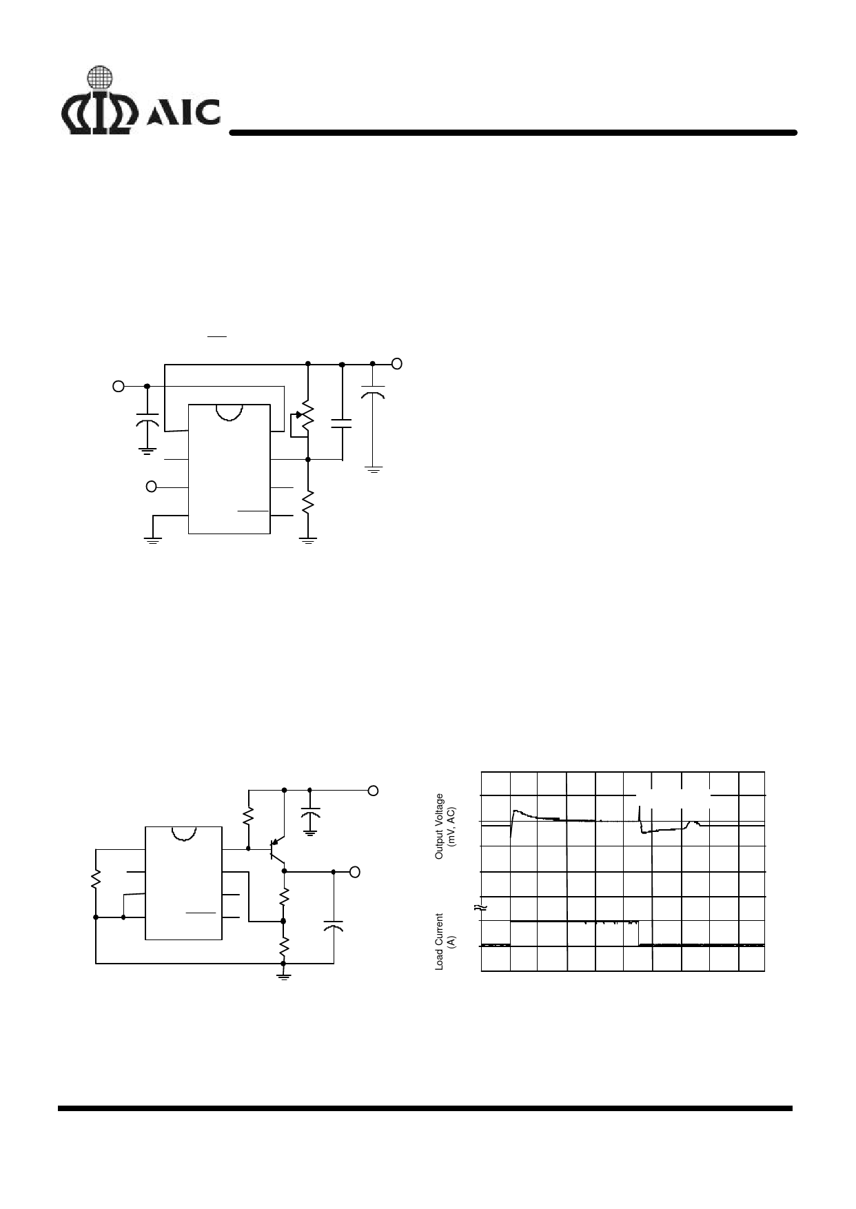
n APPLICATION EXAMPLES
Load Transient Response
VOUT=1.235(1+R1/1K)
1
VOUT
8
VIN
2
R4
SENSE
7
FB
33
3
SHDN
6
TAP
4
5
GND ERROR
AIC2951
R3
C1
+
1000µF
VIN
5V
390
6.3V
Q1
D45H2A
R1
*
C2
R2
1K
VOUT
+
1000µFx5
6.3V
100
0
-100
5
0
0
0.1 0.2
0.3
Fig. 2 Pentium® Processor Power Supply
VOUT=3.3V
0.4
0.5
0.6 0.7
0.8
Time (mS)
0.9 1.0
8
Share Link: 