BS616LV1010ACG55(2008) 查看數據表(PDF) - Brilliance Semiconductor
零件编号
产品描述 (功能)
比赛名单
BS616LV1010ACG55 Datasheet PDF : 11 Pages
| |||
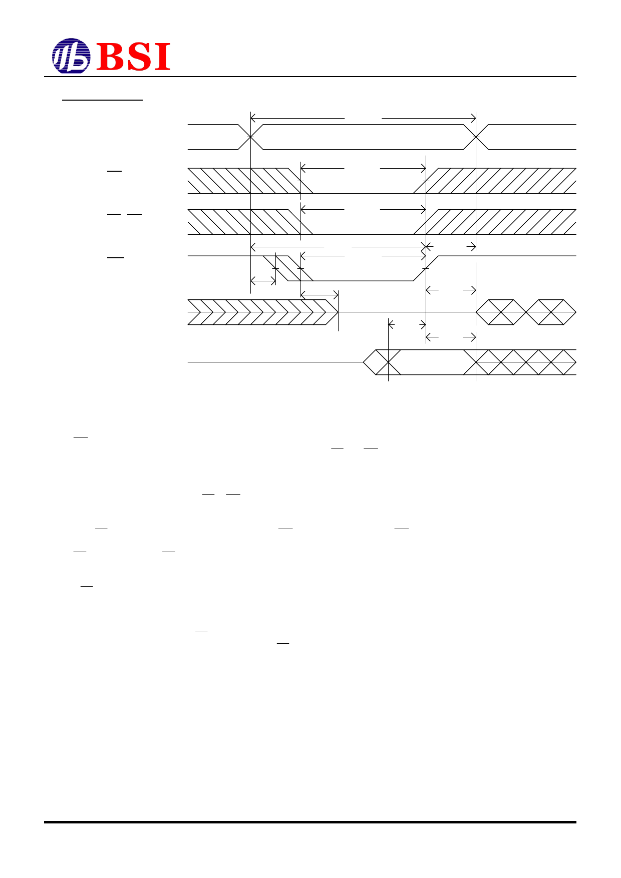
WRITE CYCLE 2 (1,6)
ADDRESS
CE
LB, UB
WE
DOUT
DIN
BS616LV1010
tWC
tCW(11)
(5)
tBW
(12)
tAW
tWP(2)
tAS
tWHZ(4,10)
tWR2(3)
tOW
(7)
(8)
tDW
tDH
(8,9)
NOTES:
1. WE must be high during address transitions.
2. The internal write time of the memory is defined by the overlap of CE and WE low. All
signals must be active to initiate a write and any one signal can terminate a write by going
inactive. The data input setup and hold timing should be referenced to the second transition
edge of the signal that terminates the write.
3. tWR is measured from the earlier of CE or WE going high at the end of write cycle.
4. During this period, DQ pins are in the output state so that the input signals of opposite
phase to the outputs must not be applied.
5. If the CE low transition occurs simultaneously with the WE low transitions or after the WE
transition, output remain in a high impedance state.
6. OE is continuously low (OE = VIL).
7. DOUT is the same phase of write data of this write cycle.
8. DOUT is the read data of next address.
9. If CE is low during this period, DQ pins are in the output state. Then the data input signals
of opposite phase to the outputs must not be applied to them.
10.Transition is measured ± 500mV from steady state with CL = 5pF.
The parameter is guaranteed but not 100% tested.
11.tCW is measured from the later of CE going low to the end of write.
12.The change of Read/Write cycle must accompany with CE or address toggled.
R0201-BS616LV1010
8
Revision 2.7
Oct.
2008
Share Link: 